Field stop type IGBT device with terminal structure and manufacturing method thereof

A technology of a terminal structure and a manufacturing method, applied in the field of IGBT devices, can solve problems such as increasing device switching loss, and achieve the effect of reducing the possibility of secondary breakdown and reducing power loss

Inactive Publication Date: 2014-11-12
WUXI NCE POWER
View PDF7 Cites 12 Cited by
  • Summary
  • Abstract
  • Description
  • Claims
  • Application Information

AI Technical Summary

Problems solved by technology

The main problems are: 1. The P+ type collector region 012 in the terminal region 02, the N type drift layer 014 and the P type main junction 021 form a PNP transistor. Generally, because the depth of the P type main junction 021 is greater than that of the P type in the cell region The depth of the body region 015, that is, the base width of the PNP transistor in the terminal region 02 is smaller than the base width of the parasitic PNP transistor in the cell region 01
The holes stored in the drift layer corresponding to the terminal region 02 will not affect the saturation voltage drop of the device, but when the device is cut off, the holes stored in the drift layer corresponding to the terminal cutoff region will be swept out by the depletion layer or compounded with electrons, increasing the switching losses of the device

Method used


Image

  • Field stop type IGBT device with terminal structure and manufacturing method thereof
  • Field stop type IGBT device with terminal structure and manufacturing method thereof
  • Field stop type IGBT device with terminal structure and manufacturing method thereof

Examples


Embodiment Construction

[0047] The present invention will be further described below in conjunction with specific drawings and embodiments.

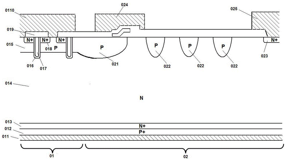
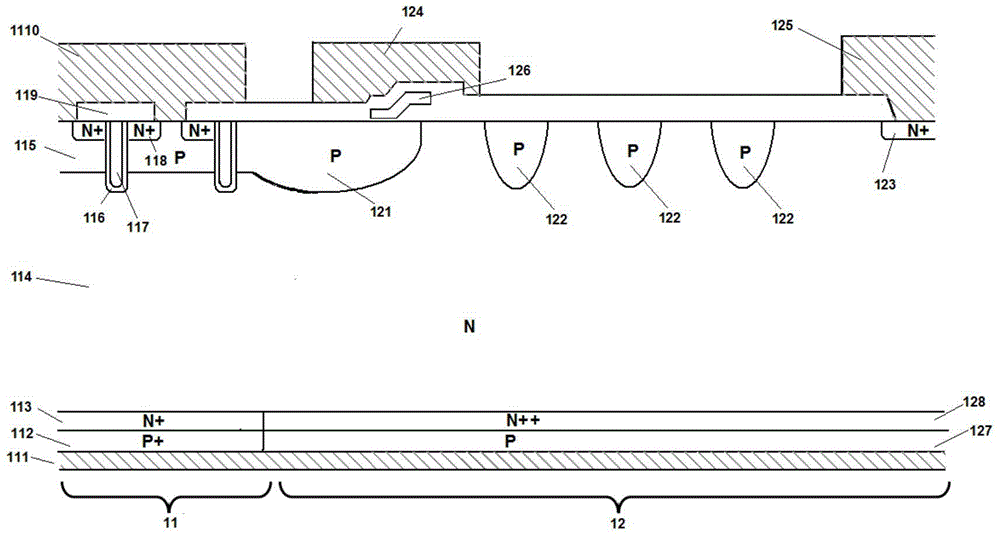
[0048] like Figure 2~Figure 10 As shown: Taking N-type field stop IGBT device as an example, the present invention includes cell region 11, terminal region 12, collector metal 111, P+ first collector region 112, N+ first buffer region 113, N-type drift region 114, P-type body region 115, gate oxide layer 116, polysilicon gate electrode 117, N+ emitter region 118, insulating dielectric layer 119, emitter metal 1110, P-type main junction 121, P-type voltage divider ring 122, N+ cut-off region 123 , gate lead-out metal 124 , cut-off metal 125 , polysilicon field plate 126 , P-type collector region 127 , N++ second buffer zone 128 , buffer mask layer 1111 and collector mask layer 1112 .

[0049] like figure 2 and Figure 10 As shown, on the top view plane of the field stop type IGBT device, it includes a cell region 11 and a terminal region 12 on the semicondu...


PUM


Abstract

The invention relates to a field stop type IGBT device with a terminal structure and a manufacturing method of the field stop type IGBT device. An IGBT device structure is arranged in a cell region of the first primary side of a semiconductor substrate, and a terminal protection structure is arranged in a terminal region of the first primary side. Collector metal making ohmic contact with a second conduction type collector region is arranged on the second primary side of the semiconductor substrate, and the second conduction type collector region is isolated from a first conduction type drifting region through a first conduction type buffer region. The second conduction type collector region comprises a second conduction type first collector region located in the cell region and a second conduction type second collector region located in the terminal region. The first conduction type buffer region comprises a first conduction type first buffer region located in the cell region and a first conduction type second buffer region located in the terminal region. According to the field stop type IGBT device, switching losses of an existing field stop type IGBT device can be effectively reduced, and use reliability of the IGBT device is improved.

Description

technical field [0001] The invention relates to an IGBT device and a manufacturing method thereof, in particular to a field-stop IGBT device with a terminal structure and a manufacturing method thereof, belonging to the technical field of IGBT devices. Background technique [0002] The insulated gate bipolar transistor IGBT (Insulated Gate Bipolar Transistor) was proposed and rapidly promoted in the 1980s. ) pushes power electronics technology to the high-frequency era, compared with other types of power semiconductors, such as bipolar transistors and MOSFETs; as a voltage control device, the insulated gate bipolar transistor can be processed with lower power loss Higher power and the ability to work in high-frequency circuits are the most prominent features and advantages of IGBTs. IGBT has been widely used in the field of power electronics. [0003] IGBT devices are generally divided into three types: punch-through type (PT type), non-punch-through type (NPT), and field-...

Claims


Application Information

Patent Timeline
Patent Type & Authority Applications(China)
IPC IPC(8): H01L29/739H01L29/06H01L29/08H01L21/331
CPCH01L29/7393H01L29/0615H01L29/66325
Inventor 朱袁正李宗清
Owner WUXI NCE POWER
Why Eureka
Try Eureka