Bonding pad structure of SMT component, installation method and circuit board
A technology of pads and parts, which is applied in the field of pad structure, mounting method and circuit board, so as to avoid bad effects
- Summary
- Abstract
- Description
- Claims
- Application Information
AI Technical Summary
Problems solved by technology
Method used
Image
Examples
Embodiment Construction
[0042] In order to make the technical problems, technical solutions and beneficial effects to be solved by the present invention clearer, the present invention will be further described in detail below in conjunction with the accompanying drawings and embodiments. It should be understood that the specific embodiments described here are only used to explain the present invention, not to limit the present invention.
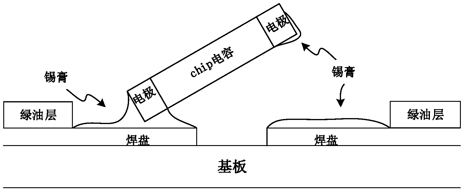
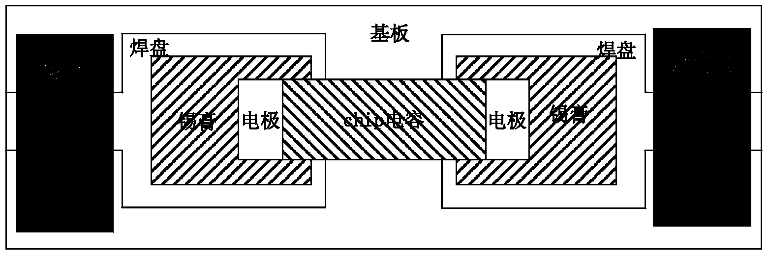
[0043] see Figure 10 , Figure 11-1 with Figure 11-2 , the mounting method of the SMT part in the preferred embodiment of the present invention, the SMT part 10 includes a body, and the first electrode 11 and the second electrode 12 arranged at the opposite ends of the body, the mounting method includes:
[0044] In step S110 , at least two pads for soldering the SMT parts 10 are provided on the surface of a substrate 20 . In this embodiment, it includes a first pad 31 and a second pad 31 for welding the first electrode 11 and the second electrode 12 respectiv...
PUM
 Abstract
Description
Claims
Application Information


