Flash memory and a reading method thereof

A flash memory and flash memory cell technology, applied in information storage, static memory, read-only memory, etc., can solve the problems of large dynamic current, long charging and discharging time, and high reading power consumption, and achieve fast reading speed and large reading. Current, the effect of improving the reading efficiency

Active Publication Date: 2014-11-19
INTEGRATED SILICON SOLUTION SHANGHAI
View PDF4 Cites 8 Cited by
  • Summary
  • Abstract
  • Description
  • Claims
  • Application Information

AI Technical Summary

Problems solved by technology

[0017] The object of the present invention is to provide a kind of flash memory and reading method thereof, 3T PMOS flash memory of the present invention can improve the read efficiency of flash memory as a whole, effectively reduce reading power consumption, overcome existing 2T PMOS flash memory tube in the read operation Disadvantages of long charging and discharging time, excessive dynamic current, and high reading power consumption

Method used


Image

  • Flash memory and a reading method thereof
  • Flash memory and a reading method thereof
  • Flash memory and a reading method thereof

Examples


Embodiment Construction

[0032] In the following description, many technical details are proposed in order to enable readers to better understand the application. However, those skilled in the art can understand that without these technical details and various changes and modifications based on the following implementation modes, the technical solution claimed in each claim of the present application can be realized.

[0033] In order to make the purpose, technical solution and advantages of the present invention clearer, the following will further describe the implementation of the present invention in detail in conjunction with the accompanying drawings.

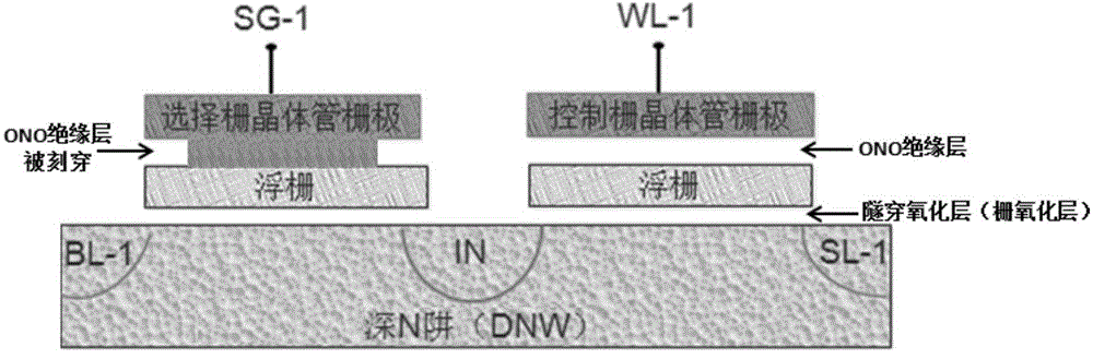
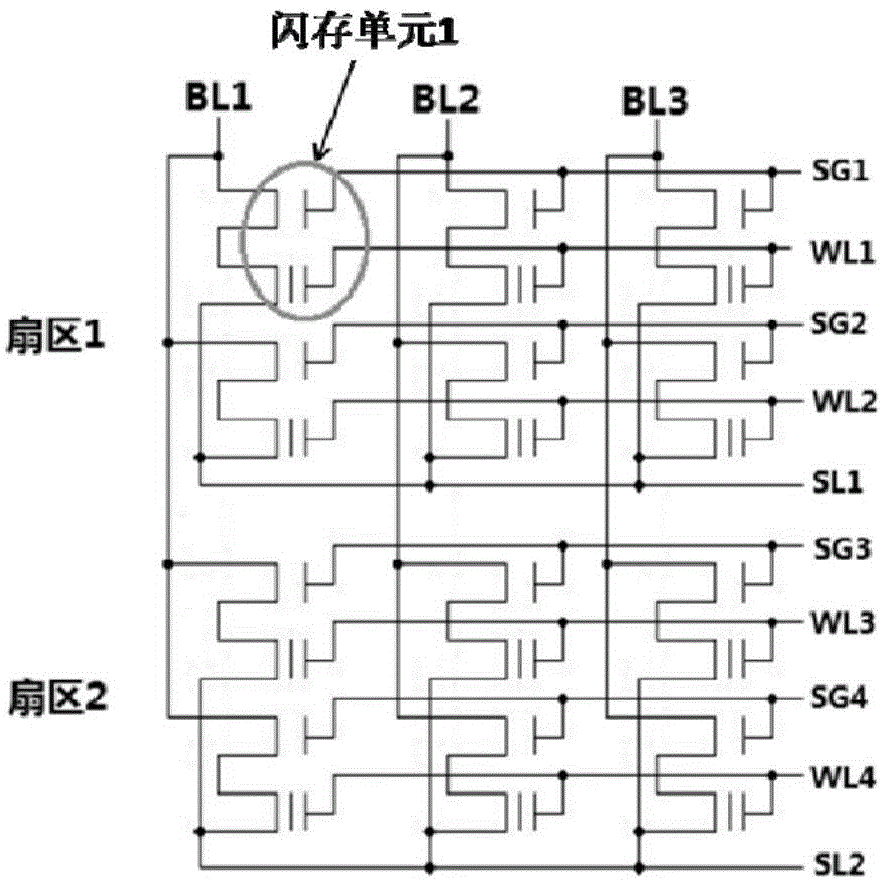
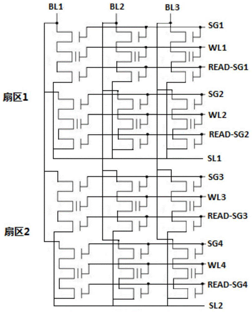
[0034]In each embodiment of the present invention, in order to be consistent with common terms in the field and to facilitate understanding of the present invention, the first control line is called a bit line (BL), and the second control line is called a select gate line (SG). The third control line is called a source line (SL), the fourth contro...


PUM


Abstract

The invention relates to a semiconductor device, and discloses a flash memory and a reading method thereof. In the invention, each flash memory unit in the flash memory includes a selection grid PMOS transistor, a control grid PMOS transistor and a reading selection grid PMOS transistor. The selection grid PMOS transistor, the control grid PMOS transistor and the reading selection grid PMOS transistor are in series connection through a first electrode and a second electrode; the absolute values of electrical thickness, channel length and threshold voltage of a grid oxide layer of the reading selection grid PMOS transistor are less than the corresponding values of the selection grid PMOS transistor. The 3T PMOS flash memory provided by the invention is dedicated to the reading select grid PMOS transistor, can improve the reading efficiency overall, effectively reduce the read power, and overcome the defects of long charge and discharge time, high dynamic current and high reading power consumption of the existing 2T PMOS flash memory in reading operations.

Description

technical field [0001] The invention relates to a semiconductor device, in particular to a flash memory and a reading method thereof. Background technique [0002] The existing embedded 2T pMOS flash memory array is composed of repeatedly arranged 2T pMOS flash memory cells. The basic structure of the flash memory cells is as follows: figure 1 shown. A 2T PMOS flash memory cell is formed by a select gate PMOS transistor (the gate potential of which is controlled by gate line SG-1) and a control gate PMOS transistor (whose gate potential is controlled by word line WL-1) connected in series. The main process parameters of the select gate PMOS transistor are as follows: "The electrical thickness of the gate oxide layer is 8nm-11nm, and the channel length is 100nm-300nm". The main process parameters of the control gate PMOS transistor are as follows: the electrical thickness of the gate oxide layer is 8nm~11nm (formed synchronously with the gate oxide layer of the selection ga...

Claims


Application Information

Patent Timeline
Patent Type & Authority Applications(China)
IPC IPC(8): G11C16/06H01L27/115
Inventor 张有志林志光陶凯宁丹谢健辉沈安星
Owner INTEGRATED SILICON SOLUTION SHANGHAI
Why Eureka
Try Eureka