White-light LED chip and manufacturing method for white-light LED chip

An LED chip and manufacturing method technology, applied in electrical components, circuits, semiconductor devices, etc., can solve the problems of easily polluted LED chip electrodes, poor welding of white LED chips, etc., so as to improve luminous efficiency, avoid easy production and processing, and avoid pollution. Effect

Active Publication Date: 2014-11-26
APT ELECTRONICS
View PDF9 Cites 12 Cited by
  • Summary
  • Abstract
  • Description
  • Claims
  • Application Information

AI Technical Summary

Problems solved by technology

[0004] The object of the present invention is to provide a white light LED chip and a method for making the white light LED chip, so as to solve the problem of poor welding of the white light LED chip in the post-process of the white light LED chip and the luminous uniformity of the white light LED chip due to the easy pollution of the electrodes of the LED chip in the existing manufacturing process The problem

Method used


Image

  • White-light LED chip and manufacturing method for white-light LED chip
  • White-light LED chip and manufacturing method for white-light LED chip
  • White-light LED chip and manufacturing method for white-light LED chip

Examples


Embodiment 1

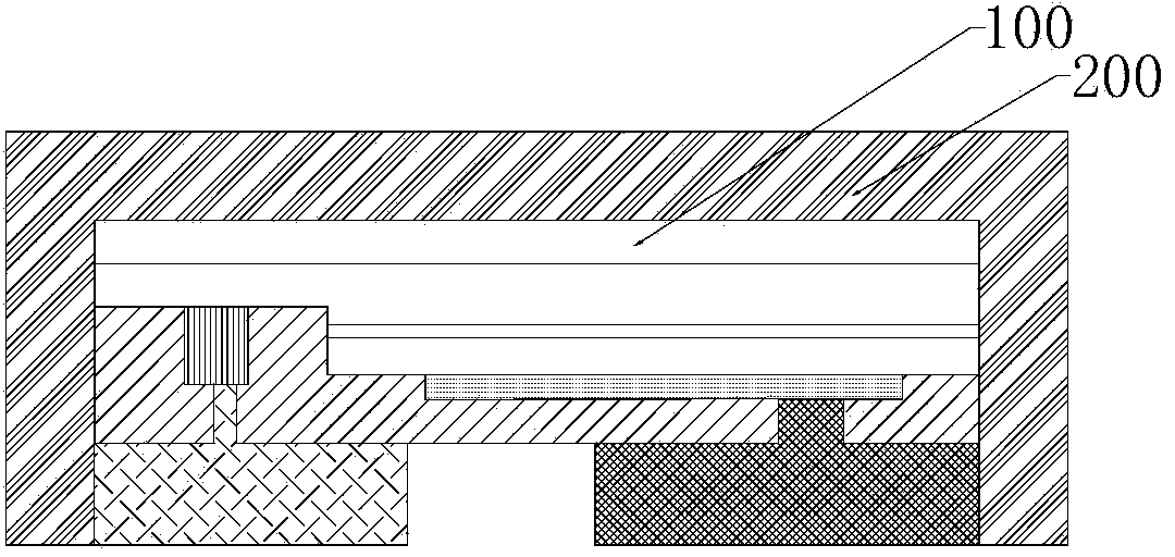
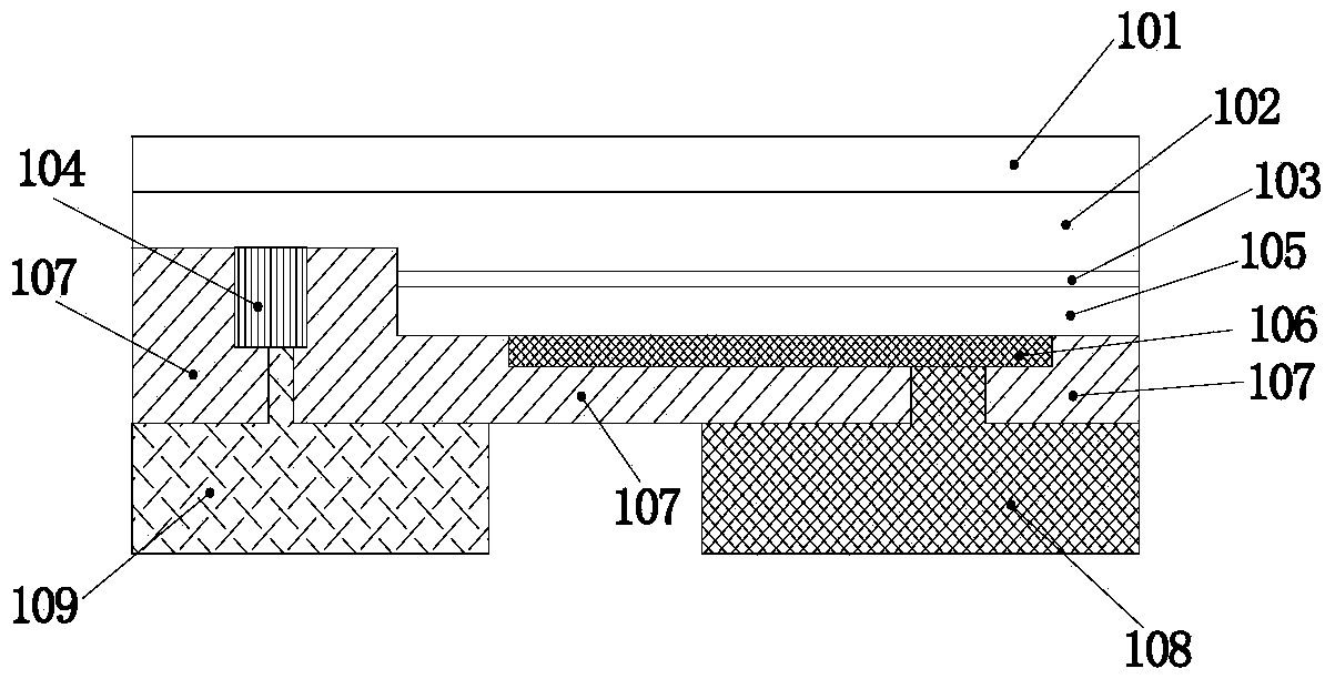
[0058] Such as Figure 1b As shown, the mounted LED chip 100 selected in this embodiment is a flip-chip LED chip, which includes an epitaxial substrate layer 101, an N-type gallium nitride layer 102 grown on the upper surface of the epitaxial substrate layer 101, and an N-type gallium nitride layer 102 grown on the epitaxial substrate layer 101. The light-emitting layer 103 on the upper surface of the N-type gallium nitride layer 102, the N-type ohmic contact layer 104 grown on the upper surface of the N-type gallium nitride layer 102, and the P-type nitrogen grown on the upper surface of the light-emitting layer 103 The gallium nitride layer 105 and the P-type ohmic contact layer 106 grown on the upper surface of the P-type gallium nitride layer 105, the P-type gallium nitride layer 105, the P-type ohmic contact layer 106, and the N-type gallium nitride layer Layer 102 and N-type ohmic contact layer 104 are also provided with an insulating layer 107 on the upper surface of th...

Embodiment 2

[0070] Such as figure 2 , as shown in Fig. 9, Fig. 10 and Fig. 11, the difference between this embodiment and Embodiment 1 is that the white light LED chip described in this embodiment is a front-mounted LED chip, which includes an epitaxial substrate layer, grown on the epitaxial substrate layer The N-type gallium nitride layer on the upper surface of the bottom layer, the light-emitting layer grown on the upper surface of the N-type gallium nitride layer part, the N-type ohmic contact layer on the upper surface of the N-type gallium nitride layer part, the The P-type gallium nitride layer on the upper surface of the light-emitting layer and the P-type ohmic contact layer on the upper surface of the P-type gallium nitride layer, a transparent conductive layer covering the P-type ohmic contact layer of the first LED chip, and a The insulating layer covers part of the surface of the first transparent conductive layer, and the first and second metal pads are respectively arrang...

Embodiment 3

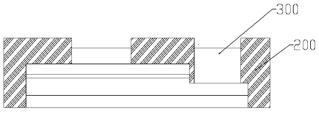
[0074] Such as image 3 , as shown in Figure 12, Figure 13 and Figure 14, the difference between this embodiment and Embodiment 1 is that the white LED chip is a vertical LED chip, which includes a metal substrate layer, bonded on the metal substrate layer The P-type gallium nitride layer on the upper surface, the light-emitting layer grown on the upper surface of the P-type gallium nitride layer, the N-type gallium nitride layer grown on the upper surface of the light-emitting layer, and the N-type gallium nitride layer grown on the N-type nitrogen An N-type ohmic contact layer on the upper surface of the gallium chloride layer. The N-type ohmic contact layer is provided with a metal pad.

[0075] The difference between the manufacturing method of the white light LED chip of this embodiment and the first embodiment is as follows: a plurality of LED chip mounting cavities with openings are formed by stamping the vertical type LED chips. The opening pattern is used for electrod...


PUM


Abstract

The invention discloses a white-light LED chip and a manufacturing method for the white-light LED chip. The white-light LED chip comprises a surface-mount type LED chip body and a light conversion layer which is used for converting light colors and formed in a prefabricated mode. The manufacturing method for the white-light LED chip includes the following steps: manufacturing the light conversion layer which is used for converting the light colors and formed in the prefabricated mode, arranging one or more installation cavities, where the LED chip bodies are installed, in the surface of the light conversion layer, arranging the LED chip bodies into the installation cavities in a surface-mount mode, and cutting the light conversion layer to form the single while-light LED chips with each installation cavity where the corresponding LED chip body is installed as the unit. By means of the white-light LED chip and the manufacturing method, the light emitting efficiency of the while-light LED chip can be improved, pollution to an electrode at the bottom of an LED chip body in an existing method can be avoided, and the white-light LED chip has the advantages of being easy to produce and manufacture and high in product yield.

Description

technical field [0001] The invention belongs to the technical field of LEDs, and in particular relates to a white LED chip and a manufacturing method thereof. Background technique [0002] White light LED chips are LED chips that can directly emit white light using Chip Scale Package (hereinafter referred to as "CSP") technology. This type of chip has the advantages of small size, large luminous angle, high current drive resistance, low manufacturing cost, and convenient downstream. Customer lighting design and other advantages. [0003] The common structural features of current LED white light chips include: flip-chip structure, electrodes are arranged at the bottom, and phosphor powder is coated on the upper surface and four sides. The phosphor layer on the upper surface and four sides is generally realized by molding and pressing semi-cured phosphor sheet technology, and the phosphor layer on the upper surface and four sides is an integrally formed structure of the same ...

Claims


Application Information

Patent Timeline
Patent Type & Authority Applications(China)
IPC IPC(8): H01L33/48H01L33/50H01L33/62
CPCH01L33/505H01L2933/0041H01L33/44H01L33/62H01L33/32H01L33/501H01L2933/0033
Inventor 万垂铭姜志荣吴倚辉姚述光曾照明肖国伟
Owner APT ELECTRONICS
Why Eureka
Try Eureka