Wave aberration detection device for optical system

An optical system and detection device technology, which is applied in the direction of photographic plate-making process exposure device, test optical performance, microlithography exposure equipment, etc., can solve the problems of poor image plane contrast and low light energy energy, etc., to eliminate errors and increase detection Light energy, the effect of improving the detection accuracy

Inactive Publication Date: 2014-12-03
INST OF OPTICS & ELECTRONICS - CHINESE ACAD OF SCI
View PDF5 Cites 12 Cited by
  • Summary
  • Abstract
  • Description
  • Claims
  • Application Information

AI Technical Summary

Problems solved by technology

[0007] In order to overcome the defects of the detection device in the above-mentioned patents and improve the detection accuracy, the purpose of the present invention is to provide an optical system wave aberration measurement device, which can eliminate the low light energy energy, poor contrast of the image plane, and the spherical surface received by the plane detector during the detection process. Receive errors and other shortcomings caused by interference fields, thereby improving detection accuracy and reducing detection time

Method used


Image

  • Wave aberration detection device for optical system
  • Wave aberration detection device for optical system
  • Wave aberration detection device for optical system

Examples


Embodiment Construction

[0025] The present invention will be described in further detail below in conjunction with the accompanying drawings and specific embodiments.

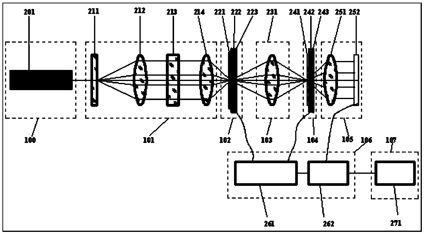
[0026] In the DUV exposure optical system, the light source 101 is generally ArF and KrF excimer lasers, and the emitted wavelengths are 193nm and 248nm respectively; Use other lasers.

[0027] The illumination module 101 includes a scattering plate 211, a collimating lens group 212, a polarizing device 213, and a focusing lens group 214, which have the functions of eliminating laser speckle, reducing the spatial coherence of the laser beam, collimating the beam, adjusting polarization characteristics, and uniform illumination. Such as figure 1 As shown, the laser beam emitted by the light source 201 enters the lighting module 102 and is diffused through the diffusion plate 211 . The scattering plate 211 diverges the laser beam, eliminates laser speckle phenomenon, reduces laser spatial coherence, and improves beam uniformity. The...


PUM


Abstract

The invention discloses a wave aberration detection device for an optical system. According to the wave aberration detection device, lights emitted by a light source are evenly projected onto an object plane of the optical system by virtue of an illumination module. A pinhole array is positioned on the object plane of the optical system, and has the functions of spatial extension and spatial division. A shearing grating is installed on an image plane of the optical system. The function of phase shift can be realized by means of driving the shearing grating to move horizontally by a fine moving stage. By virtue of a collimating optical lens group, the concentric spherical wave shearing carrying the wave aberration information of the optical system is converted to plane wave shearing. The shearing interferogram light field information in the process of phase shift is recorded by a detector. By virtue of the pinhole array, the luminous energy of the detected system is improved; by virtue of the grating, shearing interference is realized; phase shift is performed by the horizontal movement of the grating; the sphere interference is converted to plane interference by virtue of the collimating optical lens group, so that the error happening when a plane detector receives sphere interference is eliminated and therefore, the wave aberration of the optical system can be detected at high precision.

Description

technical field [0001] The invention relates to a wave aberration detection device of an optical system, in particular to high-precision detection of wave aberration of a photolithography projection objective lens. Background technique [0002] Optical lithography is the most dominant production method of modern VLSI. With the development of needs, optical projection lithography is currently the most effective method for large-scale and low-cost production of large-scale integrated circuits. This technology has high production efficiency and mature and stable technology. Widely used in flat panel display, semiconductor lighting and other semiconductor industries. With the development of very large scale integration (VLSI), its integration level is getting higher and higher, and its key dimensions are becoming smaller and smaller. Now the key dimensions of mainstream electronic products are all at 28nm, and they are developing towards 22nm large-scale and low-cost. . This ...

Claims


Application Information

Patent Timeline
Patent Type & Authority Applications(China)
IPC IPC(8): G03F7/20G01M11/02
Inventor 吕保斌邢延文林妩媚刘志祥
Owner INST OF OPTICS & ELECTRONICS - CHINESE ACAD OF SCI
Why Eureka
Try Eureka