Array substrate and preparation method thereof, and display device

An array substrate and pixel electrode technology, which is used in semiconductor/solid-state device manufacturing, electrical components, and electrical solid-state devices, etc., can solve the problems of inability to conduct data signals, the difference in etching rates between Cu and the barrier layer, and the poor uniformity of gap size. To achieve the effect of improving the yield rate

Active Publication Date: 2014-12-03
BOE TECH GRP CO LTD +1
View PDF4 Cites 12 Cited by
  • Summary
  • Abstract
  • Description
  • Claims
  • Application Information

AI Technical Summary

Problems solved by technology

[0008] In view of this, in order to solve the above problems, the embodiments of the present invention provide an array substrate and its preparation method, and a display device. The array substrate can avoid the situation where Cu is used to prepare the source, drain, and data lines , when forming the barrier layer that prevents the diffusion of Cu a

Method used


Image

  • Array substrate and preparation method thereof, and display device
  • Array substrate and preparation method thereof, and display device
  • Array substrate and preparation method thereof, and display device

Examples


Embodiment Construction

[0041] The following will clearly and completely describe the technical solutions in the embodiments of the present invention with reference to the accompanying drawings in the embodiments of the present invention. Obviously, the described embodiments are only some, not all, embodiments of the present invention. Based on the embodiments of the present invention, all other embodiments obtained by persons of ordinary skill in the art without making creative efforts belong to the protection scope of the present invention.

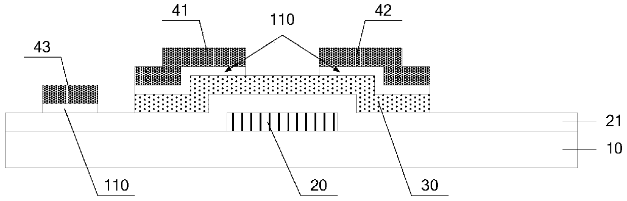
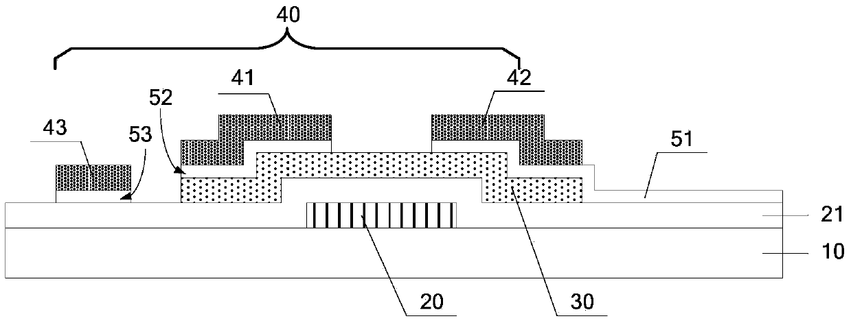
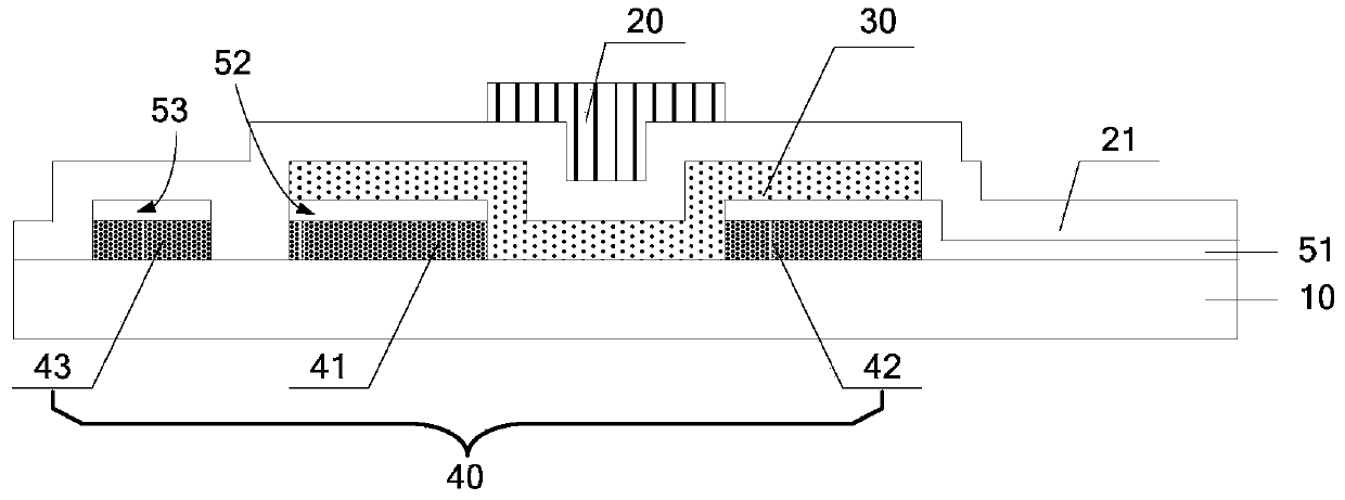
[0042] An embodiment of the present invention provides an array substrate, such as figure 2 or image 3 As shown, the array substrate includes: a gate metal layer including a gate 20, a gate line, a gate insulating layer 21, and an active layer 30 located above the base substrate 10; in addition, the array substrate also includes; The source-drain metal layer 40 of the electrode 41, the drain electrode 42, and the data line 43, the source-drain metal layer 4...


PUM


Abstract

The embodiment of the invention provides an array substrate and a preparation method thereof, and a display device, and relates to the technical field of display so that poor size uniformity of a gap between a source electrode and a drain electrode when barrier layers are formed is prevented and the cost of the barrier layers is reduced and a problem of metal loss and signal discontinuity is solved. The array substrate includes a grid metal layer which is on an underlayer substrate and includes a grid electrode and a grid line; a grid insulating layer; an active layer; a source and drain metal layer which includes the source electrode, the drain electrode, and a data line, wherein the source and drain metal layer includes a copper metal layer and/or a copper alloy layer; and a pixel electrode layer which includes a pixel electrode directly contacting the drain electrode, a first pixel electrode reservation pattern directly contacting the source electrode, and a second pixel electrode reservation pattern directly contacting the data line, wherein an area of the pixel electrode, directly contacting the drain electrode, and the first pixel electrode reservation pattern are located between the active layer and the source and drain metal layer, and an area of the pixel electrode, not directly contacting the drain electrode, and the second pixel electrode reservation pattern are located on/beneath the grid insulating layer. The preparation method is used for preparation of the array substrate.

Description

technical field [0001] The present invention relates to the field of display technology, in particular to an array substrate, a preparation method thereof, and a display device. Background technique [0002] In large-size thin film transistor liquid crystal display (Thin Film Transistor-Liquid Crystal Display, referred to as TFT-LCD), metal copper (Cu) with low resistivity is usually used as the source electrode, drain electrode, and data line material of TFT. , thereby reducing the degree of data signal delay in the array substrate. [0003] However, due to the inevitable diffusion phenomenon of Cu atoms under the action of high temperature or external electric field, that is, Cu atoms are very easy to diffuse into the active layer and other film layers (such as gate insulating layer), causing pollution to each film layer. , when the diffusion of Cu atoms is severe, it will also affect the performance of TFT devices and even lead to complete failure of device performance; ...

Claims


Application Information

Patent Timeline
IPC IPC(8): H01L27/12H01L21/77
Inventor 刘耀白金超李梁梁丁向前刘晓伟郭总杰陈曦
Owner BOE TECH GRP CO LTD
Why Eureka
Try Eureka