Charge pump circuit and its control circuit and control method
A control circuit and charge pump technology, applied in the electronic field, can solve the problems of increasing chip area, reducing efficiency, increasing chip power consumption, etc., and achieve the effect of increasing output current, reducing equivalent internal resistance, and fast response speed
- Summary
- Abstract
- Description
- Claims
- Application Information
AI Technical Summary
Problems solved by technology
Method used
Image
Examples
Embodiment 1
[0073] figure 2 For a schematic flowchart of a control method of a charge pump circuit provided in this embodiment, see figure 2 As shown, the method mainly includes:
[0074] Step 201: Detect the difference between the output voltage and the input voltage of the charge pump circuit in real time.
[0075] In this embodiment, the input voltage Vin and the output voltage Vo are introduced into the control circuit, and the difference between the output voltage Vo and the input voltage Vin is detected in real time, which is expressed as ΔV=Vo−Vin.
[0076] Step 202: Compare the difference between the current output voltage and the input voltage with a predetermined expected value of the difference, and output an error amplification signal.
[0077] In this embodiment, an expected difference value is set according to the difference between the expected output voltage Vo and the input voltage Vin, denoted as ΔVth. When the difference between the output voltage Vo and the input ...
Embodiment 2
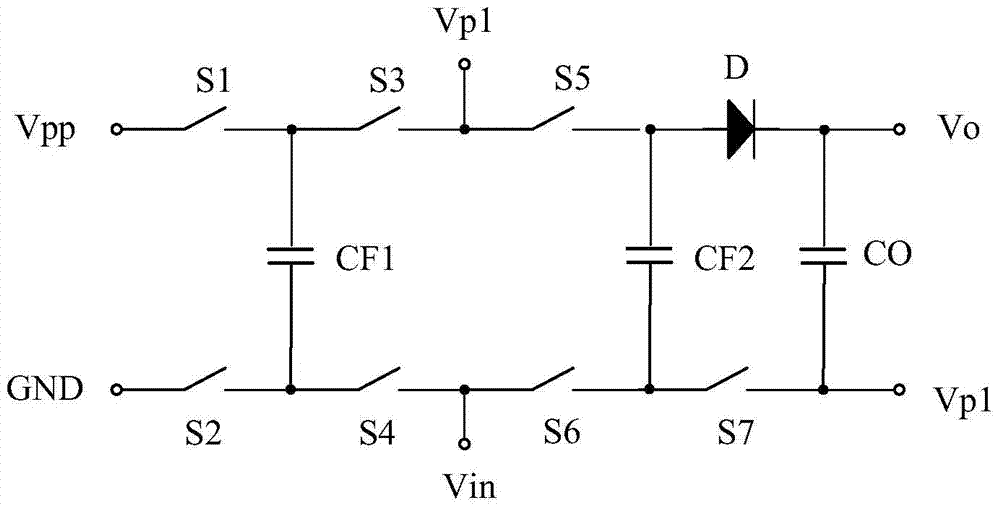
[0085] Figure 4 For a schematic structural diagram of a control circuit of a charge pump circuit provided in this embodiment, see Figure 4 As shown, the control circuit mainly includes: an error detection feedback circuit 401 , an error amplification circuit 402 , and a control voltage signal generation circuit 403 .
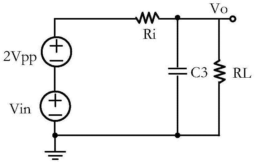
[0086] The connection relationship and working principle are that the error detection feedback circuit 401 is connected to the charge pump circuit (which can be but not limited to figure 1 or Figure 7 or image 3 As shown) the input voltage Vin and the output voltage Vo (which can be obtained by sampling, but not limited to), the error detection feedback circuit 401 detects the difference ΔV between the output voltage Vo and the input voltage Vin in real time, and outputs an error feedback signal Vb, the error The feedback signal Vb is used to represent the difference ΔV between the current output voltage Vo and the input voltage Vin, and the error feedbac...
PUM
 Abstract
Description
Claims
Application Information


