Novel optical MOS relay

A relay, a new type of technology, applied in the structural field of photorelays, can solve problems such as failure to meet high insulation requirements and damage, and achieve the effects of improving antistatic ability, increasing switching speed, and reducing dynamic loss

Inactive Publication Date: 2014-12-03
XIAMEN SILICON TOP OPTO ELECTRONICS CO LTD
View PDF5 Cites 1 Cited by
  • Summary
  • Abstract
  • Description
  • Claims
  • Application Information

AI Technical Summary

Problems solved by technology

[0007] Conventional MOSFET is an electrostatic sensitive device, its antistatic voltage is generally below 500V, and it is easily damaged by external static electricity interference
[0008] Conventional optical MOSFET structures are generally packaged in a face-to-face structure, and the dielectric withstand voltage between the input and output is generally around 2500V, which cannot meet the requirements of high-insulation industrial control applications.

Method used


Image

  • Novel optical MOS relay
  • Novel optical MOS relay
  • Novel optical MOS relay

Examples


Embodiment Construction

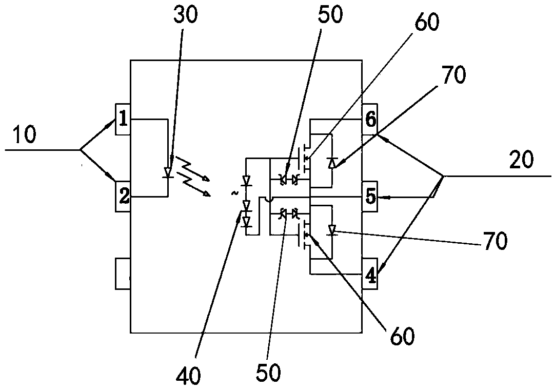
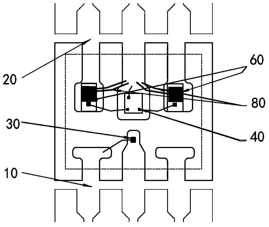
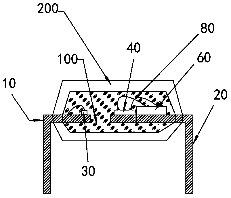
[0023] Such as figure 1 As shown, the present invention is an optical MOS relay. The input terminal 10 is composed of an infrared LED diode 30, wherein the pin1 of the input terminal 10 is connected to the "+" pole of the infrared LED diode 30, and the pin2 of the input terminal 10 is connected to the pin of the infrared LED diode 30. "-"pole;

[0024] Output terminal 2 is made up of PDA (photosensitive diode array) 40 and two MOSFET60, and each MOSFET60 is made up of the MOSFET integrated with ESD (antistatic diode) 50 and reverse recovery diode 70 respectively, wherein the "+" pole of PDA40 is connected to MOSFET60 The G pole and the "-" pole of the PDA40 are connected to the S pole of the MOSFET60; the D pole of the MOSFET60 is connected to the pin4 and pin6 of the output terminal 20, and the S pole of the MOSFET60 is connected to the pin5 of the output terminal 20, so that the S pole and the D pole of the MOSFET60 are connected to each other. become the output pin4, pin5,...


PUM


Abstract

The invention provides a novel optical MOS relay. The novel optical MOS relay is characterized in that an input end is composed of an infrared LED, a pin 1 of the input end is connected with the positive pole of the infrared LED, and a pin 2 of the input end is connected with the negative pole of the infrared LED; an output end is composed of a PDA and an MOSFET integrated with an ESD and a reverse recovery diode, the positive pole of the PDA is connected with the G pole of the MOSFET, and the negative pole of the PDA is connected with the S pole of the MOSFET; the D pole of the MOSFET is connected with a pin 4 and a pin 6 of the output end, and the S pole of the MOSFET is connected with a pin 5 of the output end; the infrared LED, the PDA, the MOSFET, the ESD and the reverse recovery diode are all located in the same plane; the input end and the output end are formed by encapsulating an inner encapsulating material and an outer-layer black encapsulating material which are made of transparent or semitransparent resin. According to the optical MOS relay, the antistatic capacity is improved, withstand voltage of media between the input end and the output end is improved, on-state and switching losses are greatly reduced, and the switching speed is also increased.

Description

technical field [0001] The invention belongs to the technical field of electrical appliances and electronics, and in particular relates to the structure of a photorelay (a solid state relay). Background technique [0002] Solid State Relays (SSR) is a non-contact electronic switch, which uses the switching characteristics of electronic components (such as switching transistors, bidirectional thyristors, MOSFETs and other semiconductor devices) to achieve non-contact and sparkless grounding. The purpose of turning on and off the circuit is to add a DC or pulse signal to its input, and the output can change from the off state to the on state (blocking state when there is no signal), that is, when the voltage is applied between the control pins , the solid state relay is turned on, and when the applied voltage between the control pins is withdrawn, the solid state relay is turned off, thereby realizing the switching function of controlling a large power load from a small power ...

Claims


Application Information

Patent Timeline
Patent Type & Authority Applications(China)
IPC IPC(8): H03K17/785
Inventor 阳琳玲
Owner XIAMEN SILICON TOP OPTO ELECTRONICS CO LTD
Why Eureka
Try Eureka