Composite type ultra-thin non-core substrate and manufacturing method thereof

A coreless substrate, composite technology, used in multilayer circuit manufacturing, semiconductor/solid-state device manufacturing, printed circuit components, etc., can solve the inner layer pattern difficulty of ultra-thin/coreless substrates, Low yield and other problems, to achieve the effect of increasing strength, reducing warpage deformation, and improving strength

Inactive Publication Date: 2014-12-03
NAT CENT FOR ADVANCED PACKAGING
View PDF4 Cites 3 Cited by
  • Summary
  • Abstract
  • Description
  • Claims
  • Application Information

AI Technical Summary

Problems solved by technology

[0004] The disadvantage of the above method is that when the inner core layer PP is very thin (generally 20-40 μm), it is very difficult to make the inner layer pattern of the ultra-thin / coreless substrate by using the conventional substrate process. When performing the horizontal line process, The substrate is easily damaged, and the substrate is warped and deformed seriously
Due to the low strength of PP, its expansion and contraction are large and uncontrolled in processes such as pressing, and the product yield is low

Method used


Image

  • Composite type ultra-thin non-core substrate and manufacturing method thereof
  • Composite type ultra-thin non-core substrate and manufacturing method thereof
  • Composite type ultra-thin non-core substrate and manufacturing method thereof

Examples


Embodiment Construction

[0021] The present invention will be further described below in conjunction with specific drawings.

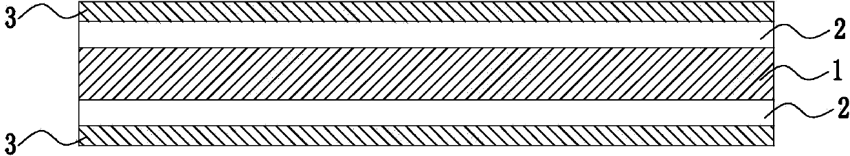
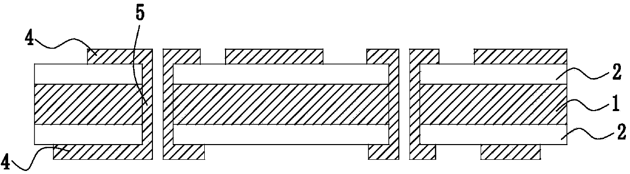
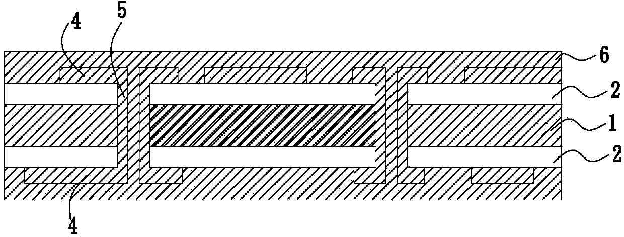
[0022] Such as Figure 5 As shown: the composite ultra-thin coreless substrate includes a PI core board. The PI core board is composed of a PI substrate 1 and copper foil 3 located on the front and back of the PI substrate 1. The copper foil 3 is bonded to the PI substrate through an adhesive layer 2 respectively. On the front and back of 1, the copper foil 3 is etched to form a core layer pattern 4; a PTH hole (metallized hole, PLATING Through Hole) 5 is set on the PI core board, and the core layer pattern 4 on the front and back of the PI core board passes through the PTH hole 5. Connection; one or more layers of PP dielectric layer 6 are respectively laminated on the front and back of the PI core board, and the PP dielectric layer 6 has an outer layer circuit pattern, and the outer layer circuit pattern is connected to the copper foil 3 .

[0023] The method for preparing ...


PUM


Abstract

The invention relates to a composite type ultra-thin non-core substrate and a manufacturing method thereof. The composite type ultra-thin non-core substrate comprises a PI core plate which comprises a PI substrate and copper foil placed on the front face and the back face of the PI substrate. The copper foil adheres to the front face and the back face of the PI substrate respectively through adhesive layers. The copper foil is subjected to etching, and core layer patterns are formed. PTHs are formed in the PI core plate. The core layer patterns on the front face and the back face of the PI core plate are connected through the PTHs. The front face and the back face of the PI core plate are respectively provided with one or more PP dielectric layers in a pressing-fitting mode. Outer layer circuit patterns are arranged on the PP dielectric layers and are connected with the copper foil. The PI substrate is used as a core layer, inner layer patterns are formed, and then manufacturing of the multi-layer substrate is achieved through a layer-adding technology. According to the method, the intensity of the core layer is greatly improved, the whole intensity of the substrate is improved, meanwhile, the PI substrate technology is mature, the thickness can meet the requirement, the method can be compatible with a common substrate technology, and extra auxiliary technologies and equipment are of no need.

Description

technical field [0001] The invention relates to a composite ultra-thin coreless (Coreless) substrate and a manufacturing method thereof, belonging to the technical field of packaging substrates. Background technique [0002] As the requirements for the size of the package become higher and higher, the requirement for the thickness of the substrate, which is an important part of the package, is also higher and higher. Ultra-thin / coreless substrates are an effective way to reduce the thickness of substrates. Typically, ultra-thin / coreless substrates use a very thin (less than 100μm, usually 20-40μm) core layer to prepare the substrate. One of the main problems is that the very thin core layer is inconvenient to process, it is very easy to damage and deform, it is incompatible with the conventional substrate processing technology in many aspects or requires additional auxiliary equipment, for example: in horizontal line processing and electroplating copper, so thin The core (...

Claims


Application Information

Patent Timeline
Patent Type & Authority Applications(China)
IPC IPC(8): H05K1/02H05K3/46H01L23/498H01L21/48
Inventor 刘文龙
Owner NAT CENT FOR ADVANCED PACKAGING
Why Eureka
Try Eureka