Image sensor and method of forming the same

An image sensor and semiconductor technology, which is applied in the field of semiconductors, can solve problems such as image halos and affect the imaging quality of image sensors, and achieve the effects of simple process methods, avoiding the appearance of halos, and improving performance

Active Publication Date: 2017-07-18
GALAXYCORE SHANGHAI
View PDF3 Cites 0 Cited by
  • Summary
  • Abstract
  • Description
  • Claims
  • Application Information

AI Technical Summary

Problems solved by technology

[0005] When the light intensity of the existing image sensor is too large, the potential well of the pixel is filled with electrons, and when the light intensity is further increased, the excess electrons will overflow outward and enter the adjacent pixel area, causing the image to appear halo Phenomenon that seriously affects the imaging quality of the image sensor

Method used


Image

  • Image sensor and method of forming the same
  • Image sensor and method of forming the same
  • Image sensor and method of forming the same

Examples


Embodiment Construction

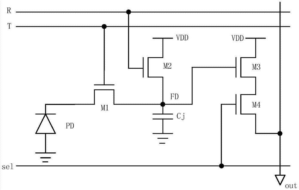
[0048] As mentioned in the background art, existing image sensors are prone to halo phenomenon, which seriously affects the imaging quality of the image sensor.

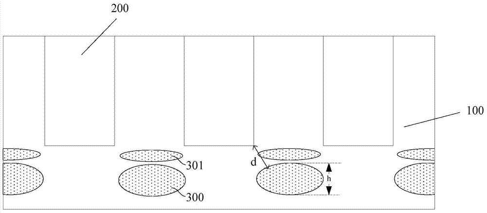
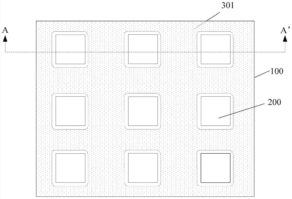
[0049] In an embodiment of the present invention, an image sensor and a method for forming the same are provided. The image sensor includes: a semiconductor substrate; several discrete photodiodes located in the semiconductor substrate, the photodiodes are arranged in a matrix; A doped isolation region beneath a portion of the semiconductor substrate between adjacent photodiodes. The doped isolation region is located in the semiconductor substrate below the photodiode, which can reduce the lateral diffusion of overflow electrons in the semiconductor substrate, thereby improving the halo phenomenon of the image sensor.

[0050] In order to make the above objects, features and advantages of the present invention more comprehensible, specific embodiments of the present invention will be described in detail below in conj...


PUM


Abstract

An image sensor and a method for forming the same, the image sensor comprising: a semiconductor substrate; a number of discrete photodiodes located in the semiconductor substrate, the photodiodes arranged in a matrix; semiconductor photodiodes located between adjacent photodiodes Doped isolation regions in the substrate. The performance of the image sensor described above is improved.

Description

technical field [0001] The invention relates to the technical field of semiconductors, in particular to an image sensor and a forming method thereof. Background technique [0002] Image sensors are semiconductor devices that convert optical image signals into electrical signals. Products with image sensors as key components have become the focus of the current and future industry, attracting investment from many manufacturers. [0003] In terms of product categories, image sensor products are mainly divided into Charge-coupled Device image sensor (CCD image sensor for short), Complementary Metal Oxide Semiconductor image sensor (CMOS sensor for short). CMOS image sensor is a fast-growing solid-state image sensor. Since the image sensor part and the control circuit part of the CMOS image sensor are integrated in the same chip, the CMOS image sensor has small size, low power consumption, and low price. Compared with The traditional CCD (Charge Coupled) image sensor has more ...

Claims


Application Information

Patent Timeline
Patent Type & Authority Patents(China)
IPC IPC(8): H01L27/146
Inventor 李杰李文强
Owner GALAXYCORE SHANGHAI
Why Eureka
Try Eureka