Tunneling transistor structure and manufacturing method thereof

A technique for tunneling transistors and manufacturing methods, which is applied in semiconductor/solid-state device manufacturing, diodes, semiconductor devices, etc., and can solve problems such as increasing the tunneling area and not increasing the on-state current of the device

Active Publication Date: 2014-12-10
HUAWEI TECH CO LTD
View PDF6 Cites 10 Cited by
  • Summary
  • Abstract
  • Description
  • Claims
  • Application Information

AI Technical Summary

Problems solved by technology

At present, tunneling field effect transistors (TFETs) generally adopt vertical tunneling, and vertical tunneling occurs in the source region and channel region under the ...

Method used


Image

  • Tunneling transistor structure and manufacturing method thereof
  • Tunneling transistor structure and manufacturing method thereof
  • Tunneling transistor structure and manufacturing method thereof

Examples


Embodiment Construction

[0050] The following will clearly and completely describe the technical solutions in the embodiments of the present invention with reference to the drawings in the embodiments of the present invention.

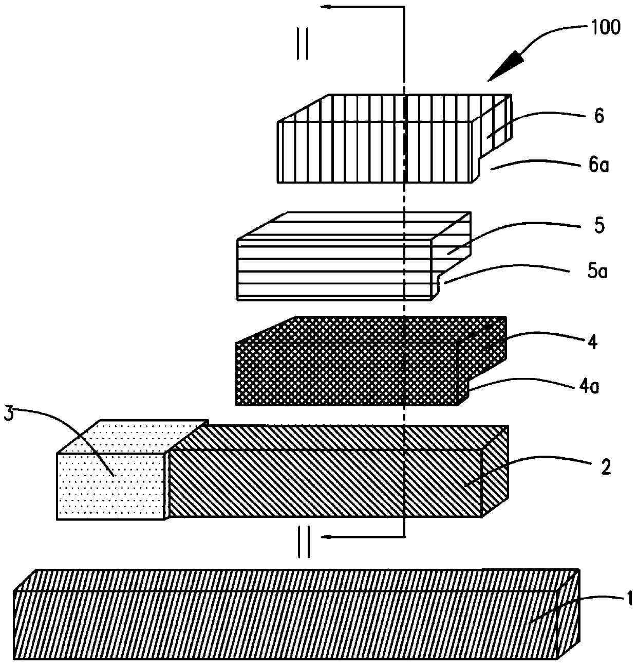
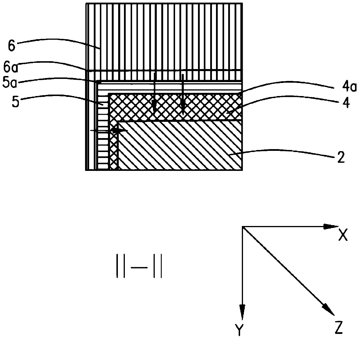
[0051] Please also refer to Figure 1 to Figure 2, is a tunneling transistor structure 100 provided in Embodiment 1 of the present invention, which includes a substrate 1, a silicon strip 2, a drain region 3, a source region 4, a gate dielectric layer 5, and a gate 6, and the silicon strip 2 is formed on one surface of the substrate 1, and the drain region 3 is formed on one side of the silicon strip 2. The source region 4 , the gate dielectric layer 5 and the gate 6 are sequentially stacked and formed on the silicon strip 2 . The source region 4 is not in contact with the drain region 3, and a first groove 4a is provided on the surface of the source region 4 facing the silicon strip 2, and the silicon strip 2 is partially housed in the first groove 4a. Inside the groove 4a....


PUM


Abstract

The invention provides a tunneling transistor structure. The tunneling transistor structure comprises a substrate, a silicon strip, a drain electrode area, a source electrode area, a gate dielectric layer and a grid electrode, wherein the silicone strip is formed on the substrate; the drain electrode area is formed at one side of the silicon strip; the source electrode area is equipped with a first groove in which the silicon strip is contained; the grate dielectric layer is formed on the source electrode area and partially covers the source electrode area; the grid electrode is equipped with a second groove in which the gate dielectric layer is contained; the cross section of the second groove is the same as that of the first groove; when in tunneling, the first groove tunnels under the effect of the second groove to form a tunneling current. The invention also provides a manufacturing method of the tunneling transistor structure. According to the tunneling transistor structure, the structures of the source electrode area and the grid electrode are changed; when in tunneling, the tunneling area of the source electrode area is expanded under the effect of the grid electrode, and point tunneling and line tunneling occur in the first groove; therefore, both the tunneling area and the tunneling portability are raised through the structure, and as a result, the on-state current of the whole device can be improved.

Description

technical field [0001] The invention relates to a tunneling transistor structure and a manufacturing method thereof. Background technique [0002] Since the birth of the first integrated circuit, integrated circuit technology has been developing along the track of "Moore's Law", and the volume of semiconductor devices has been continuously reduced. However, because the sub-threshold swing slope of the traditional metal oxide semiconductor field effect transistor (MOSFET) is limited by the thermoelectric potential, it cannot be reduced synchronously with the reduction of the device size, so that the leakage current of the device increases, and the power consumption density of the entire chip The increase seriously hinders the application of chips in system integration. Therefore, in order to improve the performance of VLSI and reduce the cost, a tunneling field effect transistor (TFET) emerges at the historic moment. [0003] Tunneling Field Effect Transistor (TFET) is esse...

Claims


Application Information

Patent Timeline
IPC IPC(8): H01L29/739H01L29/423H01L21/331
CPCH01L29/423H01L29/739H01L29/7391H01L29/42364H01L29/66356
Inventor 赵静杨喜超张臣雄
Owner HUAWEI TECH CO LTD
Why Eureka
Try Eureka