Method for improving p-type ohmic contact performance of GaN-based light-emitting device

A technology for ohmic contact and light-emitting devices, applied in semiconductor devices, electrical components, circuits, etc., can solve the difficulty of increasing p-type ohmic contacts, the difficulty of high-concentration doping of p-type GaN materials, and the ohmic contacts of p-type GaN materials need to be further improved Improvement and other issues, to achieve excellent ohmic contact characteristics, reduce the effect of height

Inactive Publication Date: 2014-12-10
SOUTH CHINA UNIV OF TECH
View PDF4 Cites 3 Cited by
  • Summary
  • Abstract
  • Description
  • Claims
  • Application Information

AI Technical Summary

Problems solved by technology

However, since the work function (7.5eV) of p-type GaN material is larger than that of ordinary metals, there is no suitable metal for p-type GaN ohmic contact; in addition, high-concentration doping of p-type GaN material is difficult, which increases the production Difficulty of good p-type ohmic contact for GaN materials
[0003] Many research groups at home and abroad are constantly exploring ways to reduce the ohmic contact of p-type GaN. However, due to the above-mentioned manufacturing difficulties, the ohmic contact of p-type GaN materials needs to be further improved.

Method used


Image

  • Method for improving p-type ohmic contact performance of GaN-based light-emitting device
  • Method for improving p-type ohmic contact performance of GaN-based light-emitting device
  • Method for improving p-type ohmic contact performance of GaN-based light-emitting device

Examples


Embodiment Construction

[0021] In order to make the objectives, technical solutions, and advantages of the present invention clearer, the present invention will be further described in detail below with reference to the accompanying drawings and embodiments, but the scope of protection of the present invention is not limited to this. If there are processes that are not specifically described below, all Those skilled in the art can refer to the prior art.

[0022] A method for improving the ohmic contact performance of p-type GaN material in this embodiment includes the following steps:

[0023] 1. Provide a GaN-based light-emitting epitaxial layer with sapphire as the base, and activate p-type GaN;

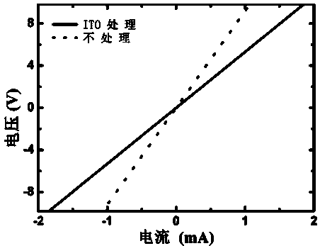
[0024] 2. Clean and process the sample, and make an indium tin oxide (ITO) layer with a thickness of 100 nm to 300 nm on the p-type GaN side;

[0025] 3. In a nitrogen environment, the sample is annealed, the annealing temperature is constant between 450°C and 550°C, and the annealing time is 1 minute to 15 minu...


PUM


Abstract

The invention discloses a method for improving the p-type ohmic contact performance of a GaN-based light-emitting device. The method comprises the following steps of: carrying out activation treatment on the p-type GaN of a GaN-based light-emitting epitaxial wafer taking sapphire as a substrate; producing an indium tin oxide ITO layer with a thickness of 100-300nm at one side of the p-type GaN; carrying out annealing treatment on a sample in a nitrogen environment, an annealing temperature being kept at 450-550 DEG C, and an annealing time being 1-15 minutes; corroding by acid solution to remove indium tin oxide ITO; carrying out a p-type GaN ohmic contact process for the traditional structure on the surface of the sample after the indium tin oxide ITO is removed, so as to complete production for a p-type contact electrode. With the adoption of the method disclosed by the invention, the binding energy of Ga2p on the surface of the p-type GaN can be reduced after ITO annealing, thus reducing the Schottky contact barrier height, therefore, obtaining for a more excellent ohmic contact characteristic is facilitated.

Description

Technical field [0001] The present invention relates to the field of semiconductor materials and devices, in particular to a method for improving the p-type ohmic contact performance of a GaN-based light-emitting device, and is suitable for GaN-based optoelectronic devices, especially for GaN-based light-emitting diodes and lasers. Background technique [0002] The third-generation semiconductor material represented by GaN has a high radiation recombination efficiency due to its direct band gap. By adjusting the doping element and the doping concentration, the light-emitting wavelength can cover the ultraviolet to the near-infrared, so as to realize RGB full-color display. Therefore, GaN-based materials are ideal materials for making visible light-emitting devices. Good ohmic contact characteristics are an important basis for realizing high-efficiency light-emitting devices. However, because the work function (7.5eV) of p-type GaN material is larger than that of general metals, ...

Claims


Application Information

Patent Timeline
Patent Type & Authority Applications(China)
IPC IPC(8): H01L33/00
CPCH01L33/005H01L33/0075
Inventor 胡晓龙王洪郑群儒赵卓立揭敢新
Owner SOUTH CHINA UNIV OF TECH
Why Eureka
Try Eureka