Interface transition layer composite structure used for P-SiC ohmic contact and preparation method thereof

A composite structure and transition layer technology, which is applied in semiconductor/solid-state device manufacturing, semiconductor devices, electrical components, etc., can solve the problems of low specific contact resistivity and difficult ohmic contact of P-type SiC materials, so as to reduce the impact and avoid The influence of tunneling mechanism and the effect of increasing carrier concentration

Inactive Publication Date: 2013-02-13
INST OF MICROELECTRONICS CHINESE ACAD OF SCI +1
View PDF8 Cites 2 Cited by
  • Summary
  • Abstract
  • Description
  • Claims
  • Application Information

AI Technical Summary

Problems solved by technology

[0006] In view of this, the main purpose of the present invention is to provide a composite structure of interfacial transition layer for P-SiC ohmic contact and its preparation method, to solve the problem of P-type SiC material ohmic contact under the condition of limited P-type doping level. Difficult problems, to achieve the purpose of repeatably obtaining low specific contact resistivity

Method used


Image

  • Interface transition layer composite structure used for P-SiC ohmic contact and preparation method thereof
  • Interface transition layer composite structure used for P-SiC ohmic contact and preparation method thereof

Examples


Embodiment

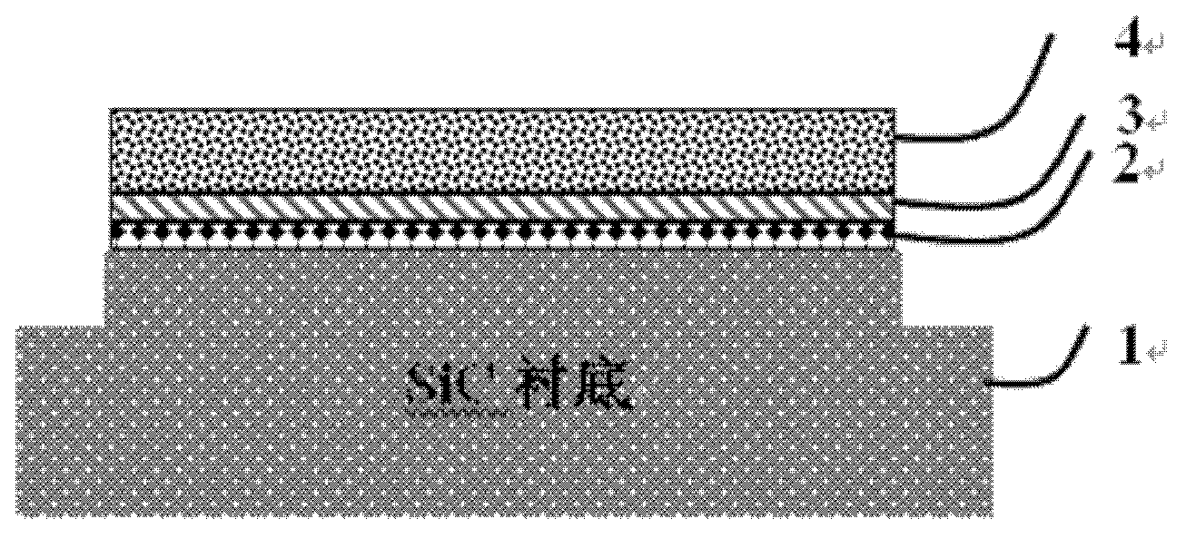
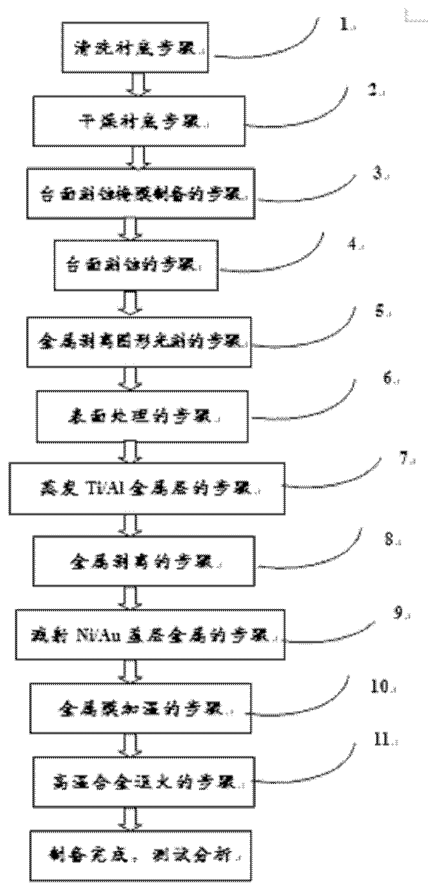
[0062] 1) Interfacial transition layer composite structure. Through the analysis of the energy band model of the composite structure of the interfacial transition layer, the selected composite structure is Al-rich layer plus Ti 3 SiC 2 carbide structure.

[0063] 2) The preparation process of the interfacial transition layer composite structure.

[0064] The main steps include: for ion implantation with a maximum energy of 550Kev (the thickness of the P-type implantation layer is about 0.7um) to activate the sample at high temperature, perform strict cleaning steps, and dry it in an oven at 120°C for 10 minutes; use 9920 photoresist , 2000rpm, produced a 3.1um thick photoresist as a mask for mesa etching; used ICP etching for 400s, and the mesa etching depth was about 0.8um; using AZ5214E ​​photoresist, produced a photoresist with a thickness of about 2.2um Peel off layer; using HF:H 2 The solution of O(1:10) corrodes about 30sec, N 2 Blow dry fully; use an evaporation ta...


PUM

PropertyMeasurementUnit
Total thicknessaaaaaaaaaa
Thicknessaaaaaaaaaa

Abstract

The invention discloses an interface transition layer composite structure used for P-SiC ohmic contact. The interface transition layer composite structure is positioned between a SiC substrate and a metal layer and comprises an enriched-Al layer and a carbide mixing layer with specific chemical composition proportion, wherein the enriched-Al layer is formed on the SiC substrate, a carbide mixing layer with specific chemical composition proportion is formed on the enriched-Al layer, and the metal layer is formed on the carbide mixing layer with specific chemical composition proportion. The invention simultaneously discloses a preparation method for the interface transition layer composite structure. By utilizing the interface transition layer composite structure provided by the invention, the height of the contact potential barrier can be adjusted effectively, the carrier concentration of a contact layer is increased, the carrier tunneling rate is increased, the good ohmic contact of the P type SiC materials can be realized effectively. Furthermore, the preparation method of the interface transition layer composite structure is simple and high in repeatability.

Description

technical field [0001] The invention relates to the field of P-type wide bandgap material ohmic contact forming technology and alloy technology, in particular to an interfacial transition layer composite structure for P-SiC ohmic contact and a preparation method thereof. Background technique [0002] The acquisition of good ohmic contact quality of wide-bandgap silicon carbide (SiC) materials is a key factor for realizing high-temperature, high-voltage, high-frequency and high-power applications of SiC devices. However, since the tunneling mass of holes is much greater than that of electrons, and the ionization energy of p-type impurities in SiC materials is higher than that of n-type impurities, it is difficult to achieve n-type doping concentration in SiC materials. The doping level of SiC, especially when ion implantation is used to form P-type doping, even if the doping concentration reaches 1E20cm -3 magnitude, but affected by activation annealing, incomplete ionizatio...

Claims


Application Information

Patent Timeline
IPC IPC(8): H01L29/45H01L21/04
Inventor 汤益丹刘可安申华军白云李博王弋宇刘新宇李诚瞻史晶晶
Owner INST OF MICROELECTRONICS CHINESE ACAD OF SCI
Why Eureka
Try Eureka