Preparation method of semi-insulating silicon carbide substrate titanium ohmic contact electrode

An ohmic contact electrode, silicon carbide substrate technology, applied in semiconductor/solid-state device manufacturing, circuits, electrical components, etc., can solve the problems of difficult technology acquisition, high cost, and high manufacturing difficulty, reducing the process flow and improving the yield. , the effect of reducing production costs

Inactive Publication Date: 2013-05-08
SHANGHAI NORMAL UNIVERSITY
View PDF5 Cites 4 Cited by
  • Summary
  • Abstract
  • Description
  • Claims
  • Application Information

AI Technical Summary

Problems solved by technology

Disadvantages: extremely difficult to produce, difficult to obtain technology, and extremely high cost
But using CVD epitaxial method to obtain highly doped n-type or p-type epitaxial layer will greatly increase the production cost

Method used


Image

  • Preparation method of semi-insulating silicon carbide substrate titanium ohmic contact electrode
  • Preparation method of semi-insulating silicon carbide substrate titanium ohmic contact electrode
  • Preparation method of semi-insulating silicon carbide substrate titanium ohmic contact electrode

Examples


Embodiment Construction

[0033] The present invention will be further described below in conjunction with specific examples.

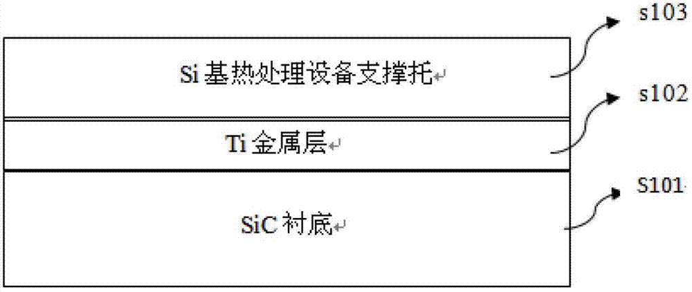
[0034] see Figure 1-Figure 2 , step s101, preparing a SiC wafer as a substrate, with a diameter of 3 inches, double-sided polishing, and carbon-side CMP;

[0035] Step s102, preparing titanium thin film electrodes, that is, using ultra-high vacuum magnetron sputtering equipment, DC target position, 80W, 300°C, 3600s, Ar gas flow 9sccm, deposition chamber pressure 0.45Pa, substrate speed 20r / min, deposition A layer of titanium electrode thin film, the thickness is controlled at 100-140nm.

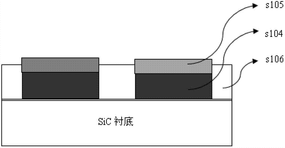
[0036] Step s103, step s104, high-temperature rapid heat treatment: the prepared titanium electrode is attached to the Si supporter of the rapid annealing furnace, and subjected to rapid heat treatment in an Ar atmosphere at 1000°C for 3 minutes to achieve an alloy compound electrode with a gradual change in Si, Ti, and SiC components.

[0037] Step s105, Au protection electrode, that is,...


PUM

PropertyMeasurementUnit
thicknessaaaaaaaaaa
surface roughnessaaaaaaaaaa

Abstract

The invention relates to a preparation method of a semi-insulating silicon carbide substrate titanium ohmic contact electrode. The preparation method is characterized by comprising the following steps that a 4H-SiC substrate is prepared; vacuum magnetron sputtering equipment is utilized, Ti electrode thin film is deposited on the 4H-SiC substrate through the magnetron sputtering equipment to form a titanium electrode; the titanium electrode is closely attached to an annealing furnace support Si base to carry out annealing heat treatment, so an alloy compound electrode with gradually varied Si, Ti and SiC components is achieved; a layer of Au is plated on the outer side of the alloy compound electrode with the gradually varied Si, Ti and SiC components and serves as electrode protection; and an SiO2 insulating layer is arranged between electrodes.

Description

technical field [0001] The invention relates to a method for preparing a semiconductor component, in particular to a method for preparing a semiconductor electrode, more specifically, a method for preparing a titanium ohmic contact electrode on a semi-insulating silicon carbide substrate, and belongs to the technical field of semiconductor electrodes . Background technique [0002] In the semiconductor industry, Si material has been developed as a dominant semiconductor device for nearly half a century. With the development of science and technology and people's pursuit of the performance of microelectronic devices, the feature size of semiconductor devices has been continuously reduced, and the size of a single transistor has gradually reached the dual limits of physics and technology. The migration of CMOS devices using traditional Si as channel materials The relative performance requirements of the rate are getting lower and lower, which can no longer meet the requiremen...

Claims


Application Information

Patent Timeline
Patent Type & Authority Applications(China)
IPC IPC(8): H01L21/04
Inventor 张永平陈之战石旺舟卢吴越谈嘉慧程越李薛
Owner SHANGHAI NORMAL UNIVERSITY
Why Eureka
Try Eureka