Substrate and base plate separation process, sacrificial layer and flexible display device and production process thereof

A flexible display and sacrificial layer technology, applied in the manufacture of semiconductor/solid-state devices, electric solid-state devices, semiconductor devices, etc., can solve the problem of easily damaged electronic devices, high temperature resistance of viscous materials, poor drug resistance, limited type of substrate application scope, etc. problem, to achieve the effect of low cost, no impact on device performance, fast device performance

Inactive Publication Date: 2014-12-10
GUANG ZHOU NEW VISION OPTO ELECTRONICS TECH
View PDF8 Cites 29 Cited by
  • Summary
  • Abstract
  • Description
  • Claims
  • Application Information

AI Technical Summary

Problems solved by technology

However, this method in the prior art has some defects: since the flexible substrate tends to directly produce strong adhesion with the hard substrate, it is often easy to damage the flexible film substrate when it is detached from the hard substrate. Films on flexible substrates and electronic devices on them
This method is simple and fast, but the viscous material has poor high temperature resistance and chemical resistance, which severely limits the scope of application of this type of substrate

Method used


Image

  • Substrate and base plate separation process, sacrificial layer and flexible display device and production process thereof
  • Substrate and base plate separation process, sacrificial layer and flexible display device and production process thereof
  • Substrate and base plate separation process, sacrificial layer and flexible display device and production process thereof

Examples


Embodiment 1

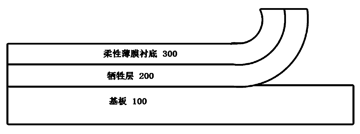
[0054] A substrate and substrate separation process for the preparation of a flexible display device, comprising the following steps:

[0055] (1) Prepare a sacrificial layer 200 on the substrate 100, and the sacrificial layer 200 is a carbon thin film.

[0056] The substrate 100 is a hard material, which can be made of glass, metal, plastic and fiber, or it can be a substrate 100 based on the above materials with a buffer layer.

[0057] Wherein, the simple carbon film is any one or more than one of amorphous carbon film, carbon nanotube film, graphene film, fullerene film or diamond-like film.

[0058]The thickness of the sacrificial layer 200 is 1nm-1000nm, and the sacrificial layer 200 is prepared by any one of chemical vapor deposition, physical vapor deposition or solution processing.

[0059] (2) Prepare the flexible film substrate 300 on the sacrificial layer 200 .

[0060] The material of the flexible film substrate 300 can be polyimide (Polyimide, PI), polyethylen...

Embodiment 2

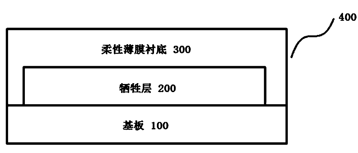
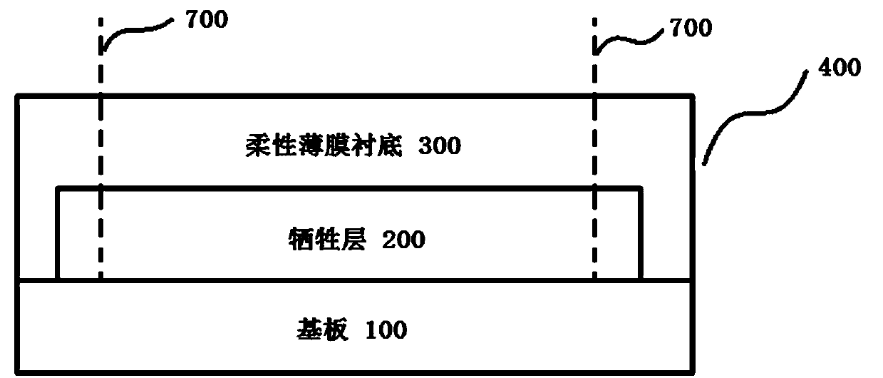
[0071] A substrate and substrate separation process for the preparation of a flexible display device, other features are the same as in Embodiment 1, the difference is that it also has the following features:

[0072] Step (2) of this embodiment prepares a flexible film substrate 300, so that the flexible film substrate 300 completely covers the sacrificial layer 200 to form a partial covering body 400, and the prepared structure is as follows figure 2 shown. The flexible film substrate 300 should completely cover the sacrificial layer 200 , the area of ​​the flexible film substrate 300 is larger than that of the sacrificial layer 200 , and the flexible film substrate 300 is in direct contact with the substrate 100 outside the edge of the sacrificial layer 200 . This structure can improve the adhesion of the flexible film substrate 300 and the sacrificial layer 200 to the substrate 100, and reduce the chance of accidental dissociation of the flexible substrate during the devi...

Embodiment 3

[0081] A substrate and substrate separation process for the preparation of a flexible display device, other features are the same as in Embodiment 1, the difference is that it also has the following features, the process specifically includes the following steps:

[0082] (1) Prepare the sacrificial layer 200 on the substrate 100 to form the first body 500 .

[0083] (2) Prepare the flexible film substrate 300, so that the flexible film substrate 300 completely covers the outer surface of the first body 500 to form a fully covered body 600, such as Figure 5 shown.

[0084] (3) Electronic components are prepared on the flexible film substrate on the side close to the sacrificial layer 200, and the flexible film substrate on the side close to the sacrificial layer 200 refers to Figure 5 Side A in . (4) Detaching the flexible film substrate 300 from the substrate 100 to obtain a finished flexible display device.

[0085] Step (4) specifically includes, such as Image 6 as s...


PUM


Abstract

Disclosed are a substrate and base plate separation process for a flexible display device and the flexible display device and a production process thereof. The substrate and base plate separation process comprises the following steps of step 1, producing a sacrificial layer on a base plate, wherein the sacrificial layer is a carbon elementary substance film; step 2, producing a flexible film substrate on the sacrificial layer; step 3, producing an electronic element on the flexible film substrate; step 4, dissociating the flexible film substrate from the base plate to obtain the flexible display device. The sacrificial layer is the carbon elementary substance film, particularly any one or more than one of an amorphous carbon film, a carbon nanotube film, a graphene thin film, a fullerene thin film or a diamond film. The thickness of the sacrificial layer is 1 to 100 nm. According to the substrate and base plate separation process, the sacrificial layer and the flexible display device and the production process thereof, the carbon elementary substance film serves as the sacrificial layer and accordingly the separation of the substrate and the base plate can be simple, low in cost and rapid and the device performance cannot be affected.

Description

Technical field [0001] The present invention involves flexible semiconductor film technology fields, especially the substrate separation process and substrate separation process of a flexible display device preparation and the sacrifice layer used, the preparation process with the flexible display device with the separation process, and through the separation process.Prepared flexible display device. Background technique [0002] When the flexible display device is prepared, the flexible thin -film substrate is formed on the hard substrate, and then the device is made on the flexible thin film substrate. Finally, the substrate and the flexible thin film substrate are removed from the removing the device to remove the substrate.However, there are some defects in the existing technology: because flexible substrates often directly produce a strong adhesion effect with the hard substrate, so the flexible thin -film substrate is often easily damaged when the flexible thinner substrate...

Claims


Application Information

Patent Timeline
Patent Type & Authority Applications(China)
IPC IPC(8): H01L51/00H01L51/56H01L51/52
CPCH01L21/7813H10K77/111Y02E10/549Y02P70/50
Inventor 徐苗许志平李洪濛邹建华王磊陶洪彭俊彪
Owner GUANG ZHOU NEW VISION OPTO ELECTRONICS TECH
Why Eureka
Try Eureka