Switching circuit capable of reducing electromagnetic interference

A switching circuit, electromagnetic interference technology, applied in the field of single live wire electronic switch, can solve problems such as adverse effects of equipment stability, damage, and electromagnetic interference harmfulness, etc., to improve anti-surge performance, reduce electromagnetic interference, and eliminate electromagnetic interference. Effect

Active Publication Date: 2014-12-10
ZHEJIANG CHINT BUILDING ELECTRICS
View PDF4 Cites 2 Cited by
  • Summary
  • Abstract
  • Description
  • Claims
  • Application Information

AI Technical Summary

Problems solved by technology

Generally, there are two ways to solve differential mode interference, one is to add a low-pass filter on the power circuit board, and the other is to add filtering processing to the switching device, but these solutions often increase the standby time of the single live wire switching circuit. Power consumption, which affects the normal performance of the product, and also leads to new defects that do not meet energy conservation and environmental protection
[0003] Electromagnetic interference is very harmful and will cause unstable operation of other electronic equipment, especially for power-type switching circuits used to control the on / off of the main circuit with loads. The main circuit is usually an AC circuit that carries a large load , so its electromagnetic interference not only cannot be ignored, but also has adverse effects on the stability of the equipment in the main circuit it controls, and even causes damage
Because the electromagnetic interference of this kind of switching circuit is very harmful, if the electromagnetic interference is not reduced, it will not only cause the instability of the local product and the degradation of the function, but also directly affect the market competitiveness of the local product, so it is received by many international / National standards restrict or even prohibit

Method used


Image

  • Switching circuit capable of reducing electromagnetic interference
  • Switching circuit capable of reducing electromagnetic interference
  • Switching circuit capable of reducing electromagnetic interference

Examples


Embodiment Construction

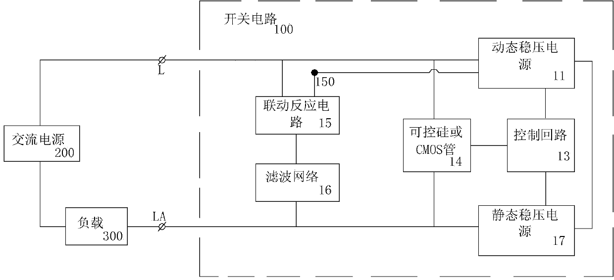
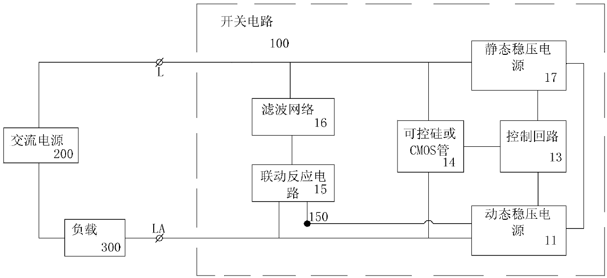
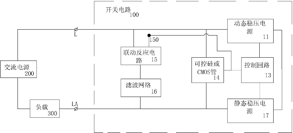
[0023] The following is attached Figures 1 to 6 The given examples describe in detail the specific implementation of the switch circuit for reducing electromagnetic interference of the present invention, and the switch circuit for reducing electromagnetic interference of the present invention is not limited to the description of the following embodiments.

[0024] Figure 1-3 They are circuit principle block diagrams of three embodiments of the switch circuit 100 for reducing electromagnetic interference of the present invention. figure 1 , 2 The circuit structure and control relationship that the DC positive pole VCC of the dynamic voltage stabilized power supply 11 provides the control voltage to the signal input terminal 150 of the linkage reaction circuit 15 are respectively shown in , wherein figure 2 Yes figure 1 The schematic block diagram of the equivalent circuit of the first embodiment shown, image 3 The figure shows the circuit structure and control relations...


PUM


Abstract

The invention discloses a switching circuit capable of reducing electromagnetic interference. The switching circuit comprises a first terminal and a second terminal which are respectively connected to an alternating current power supply and a load, a control loop which is connected between the first terminal and the second terminal, a dynamic voltage-stabilized source and a static voltage-stabilized source which are connected between the two terminals in series and are used for supplying the power to the control loop, and a controlled silicon or a CMOS (Complementary Metal Oxide Semiconductor) tube which is connected between the two terminals in series and is controlled by the control loop, wherein a current main loop of the switching circuit is formed by the first terminal, the second terminal, the control loop, the dynamic voltage-stabilized source, the static voltage-stabilized source and the controlled silicon or the CMOS tube. The switching circuit further comprises a linked switching circuit merging into the current main loop, and the linked switching circuit comprises a filter network used for reducing the electromagnetic interference and a linked reaction circuit used for controlling synchronous linkage of the filter network and the switching circuit. The switching circuit is designed for the electromagnetic interference problem caused by adopting the controlled silicon or the CMOS tube as a main loop, and provides a scheme, which is easily controlled and low in cost, and is capable of better solving the problem of electromagnetic compatibility, and the linked switching circuit is guaranteed to have no standby power consumption.

Description

technical field [0001] The invention relates to a single live wire electronic switch for household and similar fixed electrical devices, in particular to a circuit based on a single live wire electronic switch controlled by a silicon controlled rectifier or a CMOS tube. Background technique [0002] As we all know, electronic components in electrical circuits will emit electromagnetic energy and form electromagnetic interference while completing their own functions. Electronic switches (also called switching circuits) are no exception. They often use silicon controlled rectifiers or CMOS Switching semiconductor devices such as tubes, when these devices are in the working state, there are often low-frequency electromagnetic interference below 2MHz. This low-frequency electromagnetic interference can be transmitted through conduction and radiation, especially its switching action, which leads to electromagnetic interference. main cause of interference. The first terminal L of...

Claims


Application Information

Patent Timeline
Patent Type & Authority Applications(China)
IPC IPC(8): H03K17/567
Inventor 石勇张庆张宏文江冠球
Owner ZHEJIANG CHINT BUILDING ELECTRICS
Why Eureka
Try Eureka