Single-molecular-junction logic gate

A technology of molecular junctions and logic gates, applied in the field of logic devices, can solve the problems of ineffective realization, reduced computer size, no signal output capability, etc., and achieves the effect of fast operation speed, high logic operation rate and response ability.

Inactive Publication Date: 2014-12-10
SUZHOU HUALAIDE ELECTRONICS TECH
View PDF2 Cites 2 Cited by
  • Summary
  • Abstract
  • Description
  • Claims
  • Application Information

AI Technical Summary

Problems solved by technology

Further narrowing the electronic conduction line width, reducing the size of the computer, reducing the cost and power consumption, and increasing the computing speed are close to the limit in theory and technology. In recent years, scientists have been trying various nanoparticle methods and concepts, trying to replace silicon semiconductors. As the concept of logic gates, on the one hand, although there are a series of nanoparticle methods that can achieve corresponding information reading by introducing nanoparticles or light, and then have the ability to operate logic gates, this type of method cannot effectively realize microscale. The way of information input and information reading at the same time, and its information reading is highly dependent on the liquid phase environment to achieve
The concept of conductive molecular junction is a kind of semiconductor junction constructed between two electrodes based on a single organic small molecule through complexation recently proposed by scientists. This type of molecular junction has the potential to be realized as a computing unit at the molecular level. logic operation, so as to achieve the semiconductor preparation process requirements below 10 nanometers. However, the current research mainly focuses on the research on the current and voltage characteristics of molecular junctions. Therefore, although there are some reports on molecular switches, this type of molecular junction logic gates Not good signal output capability

Method used


Image

  • Single-molecular-junction logic gate
  • Single-molecular-junction logic gate
  • Single-molecular-junction logic gate

Examples


Embodiment Construction

[0016] The following will clearly and completely describe the technical solutions in the embodiments of the present invention. Obviously, the described embodiments are only some of the embodiments of the present invention, rather than all the embodiments. Based on the embodiments of the present invention, all other embodiments obtained by persons of ordinary skill in the art without making creative efforts belong to the protection scope of the present invention.

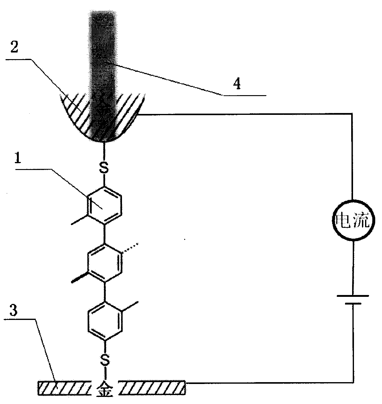
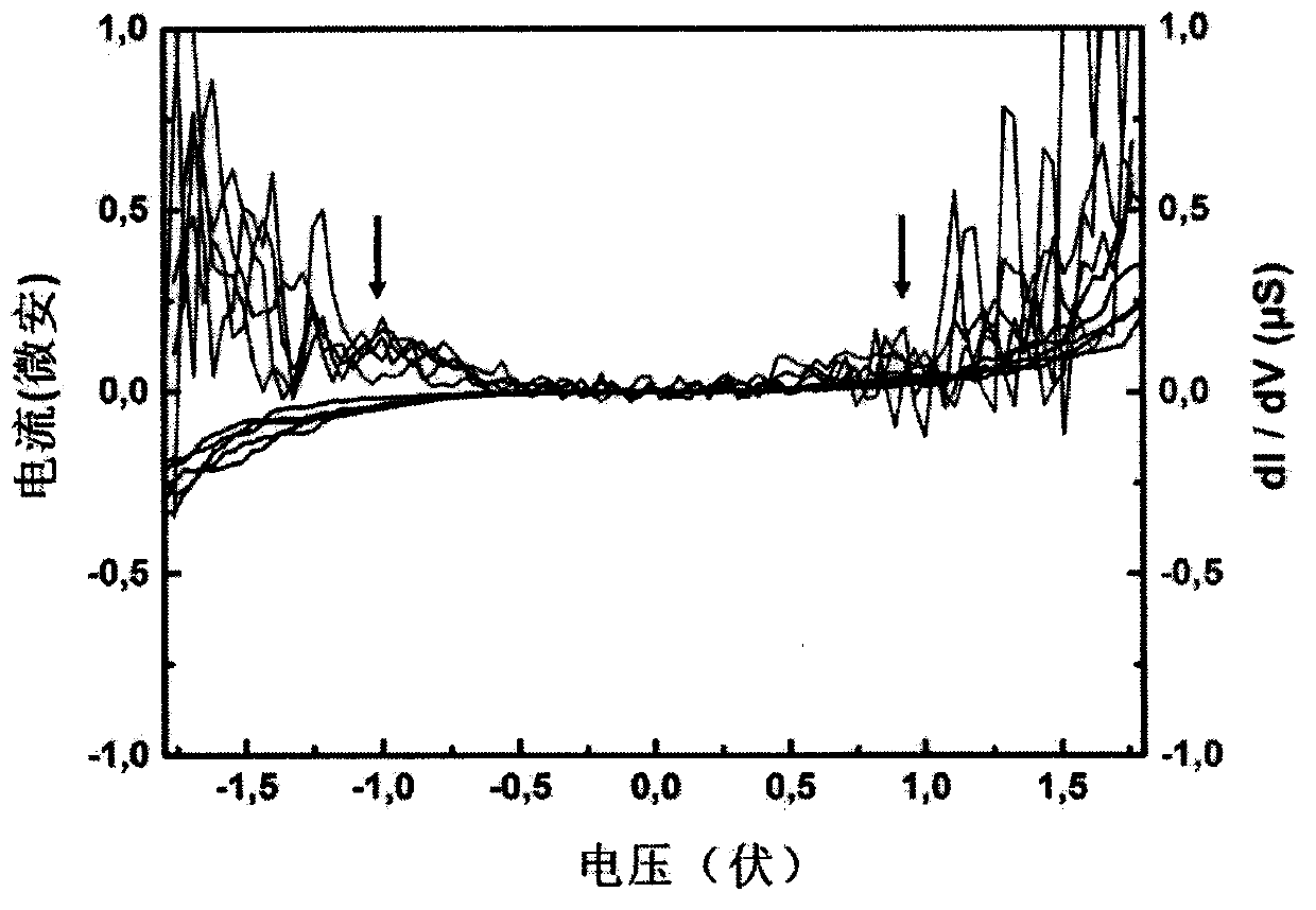
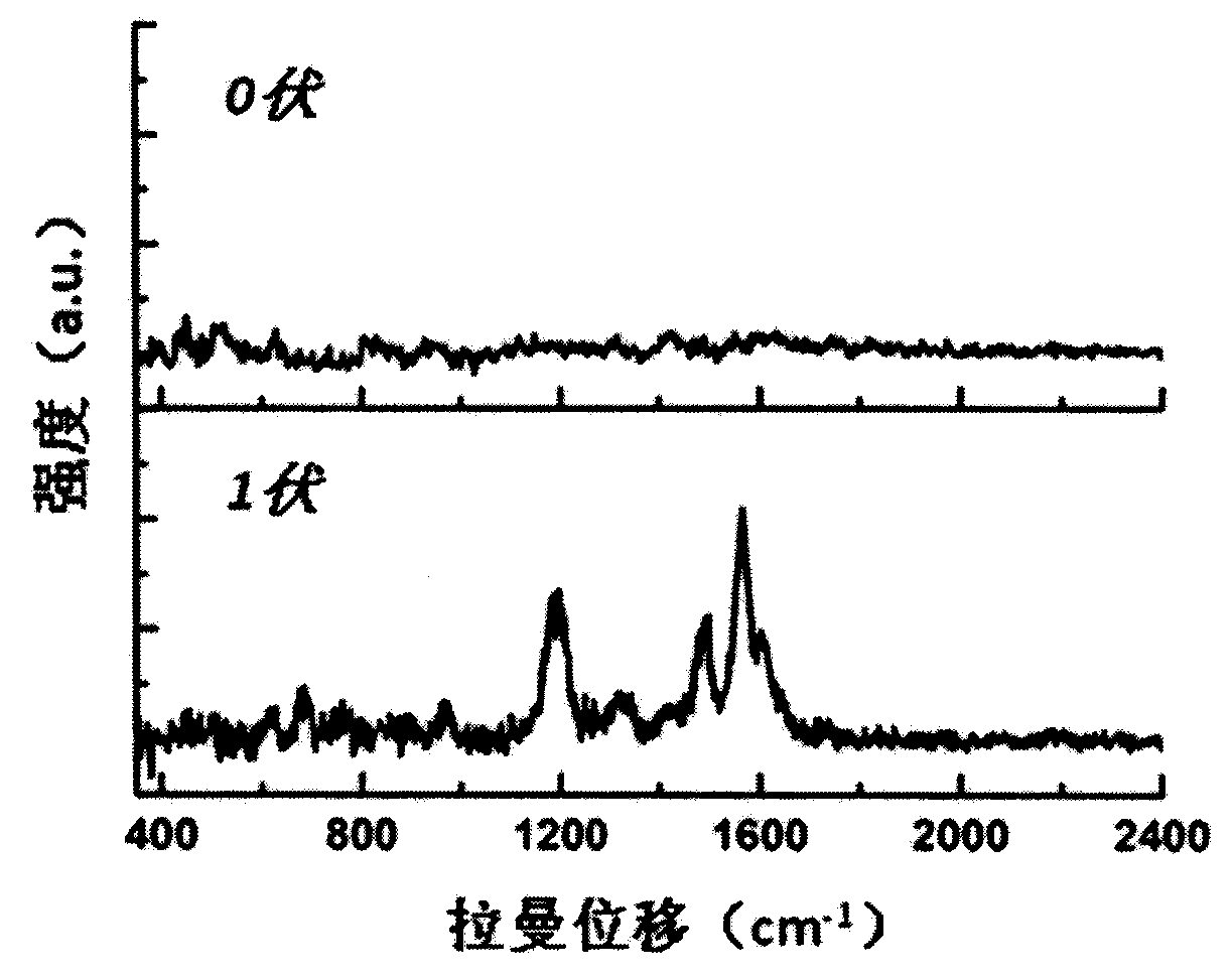
[0017] see Figure 1 to Figure 4 , the embodiment of the present invention includes:

[0018] A single-molecule junction logic gate, comprising: a logic gate single-molecule junction 1, a positive electrode 2, a negative electrode 3, a laser device 4, and a molecular junction logic gate readout device, the two ends of the logic gate single-molecule junction are respectively connected to the positive electrode 2 Electrically connected to the negative electrode 3, the laser device 4 is arranged directly above the elec...


PUM


Abstract

The invention discloses a single-molecular-junction logic gate. The single-molecular-junction logic gate comprises a logic gate single molecular junction, a positive electrode, a negative electrode, a laser device and a molecular junction logic gate readout device, wherein the two ends of the logic gate single molecular junction are electrically connected with the positive electrode and the negative electrode respectively; the laser device is arranged over the electrodes; the molecular junction logic gate readout device is arranged on one side of the logic gate single molecular junction, and is arranged close to the logic gate single molecular junction; the emitting end of the laser device points to the logic gate single molecular junction; and laser light emitted by the laser device is laser light of 633 nanometers. Logic operation of the micro-scale logic gate single molecular junction under an electrical control condition is realized, and the logic gate single molecular junction has extremely high logic operating rate and response capability; and meanwhile, real single molecular operation capability is provided by the logic gate single molecular junction, so that an important foundation is laid for the replacement of a silicon semiconductor technology.

Description

technical field [0001] The invention relates to a logic device, in particular to a single molecular junction logic gate. Background technique [0002] Logic gates are the basic components of integrated circuits. Computers that are widely used today are mainly silicon semiconductor integrated circuits. For traditional silicon semiconductor integrated circuits, their computing power is highly related to the size of the semiconductor unit. When the semiconductor is densely packed to a certain extent At this time, the circuit will produce overheating and cross-interference that are difficult to overcome. Further narrowing the electronic conduction line width, reducing the size of the computer, reducing the cost and power consumption, and increasing the computing speed are close to the limit in theory and technology. In recent years, scientists have been trying various nanoparticle methods and concepts, trying to replace silicon semiconductors. As the concept of logic gates, on ...

Claims


Application Information

Patent Timeline
Patent Type & Authority Applications(China)
IPC IPC(8): H03K19/173
Inventor 毕海
Owner SUZHOU HUALAIDE ELECTRONICS TECH
Why Eureka
Try Eureka