Front end input waveguide structure of direction coupling optical waveguide detector

A directional coupling, front-end input technology, applied in the coupling, light guiding, optics and other directions of optical waveguides, can solve the problems of weak propagation direction, uneven photocurrent distribution of waveguide detectors, uneven photocurrent distribution, etc., to increase the photocurrent , Overcome the shortcomings of the horizontal coupling waveguide detector, and solve the effect of overheating and burning

Inactive Publication Date: 2014-12-24
UNIV OF ELECTRONICS SCI & TECH OF CHINA
View PDF5 Cites 13 Cited by
  • Summary
  • Abstract
  • Description
  • Claims
  • Application Information

AI Technical Summary

Problems solved by technology

[0007] The existing problems of waveguide detectors are: the distribution of photocurrent along the waveguide is uneven, it is exponentially attenuated, and the coupling loss is large; the photocurrent is very strong at the front end of the waveguide, and gradually weakens in the direction of propagation, and the front end of the waveguide determines the photocurrent. saturation value, which limits the incident optical power
[0008] In 2008, in order to solve the problem of uneven photocurrent distribution and large coupling loss of waveguide

Method used


Image

  • Front end input waveguide structure of direction coupling optical waveguide detector
  • Front end input waveguide structure of direction coupling optical waveguide detector
  • Front end input waveguide structure of direction coupling optical waveguide detector

Examples


Embodiment

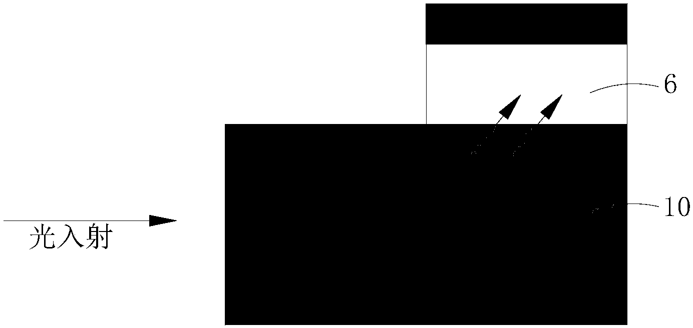
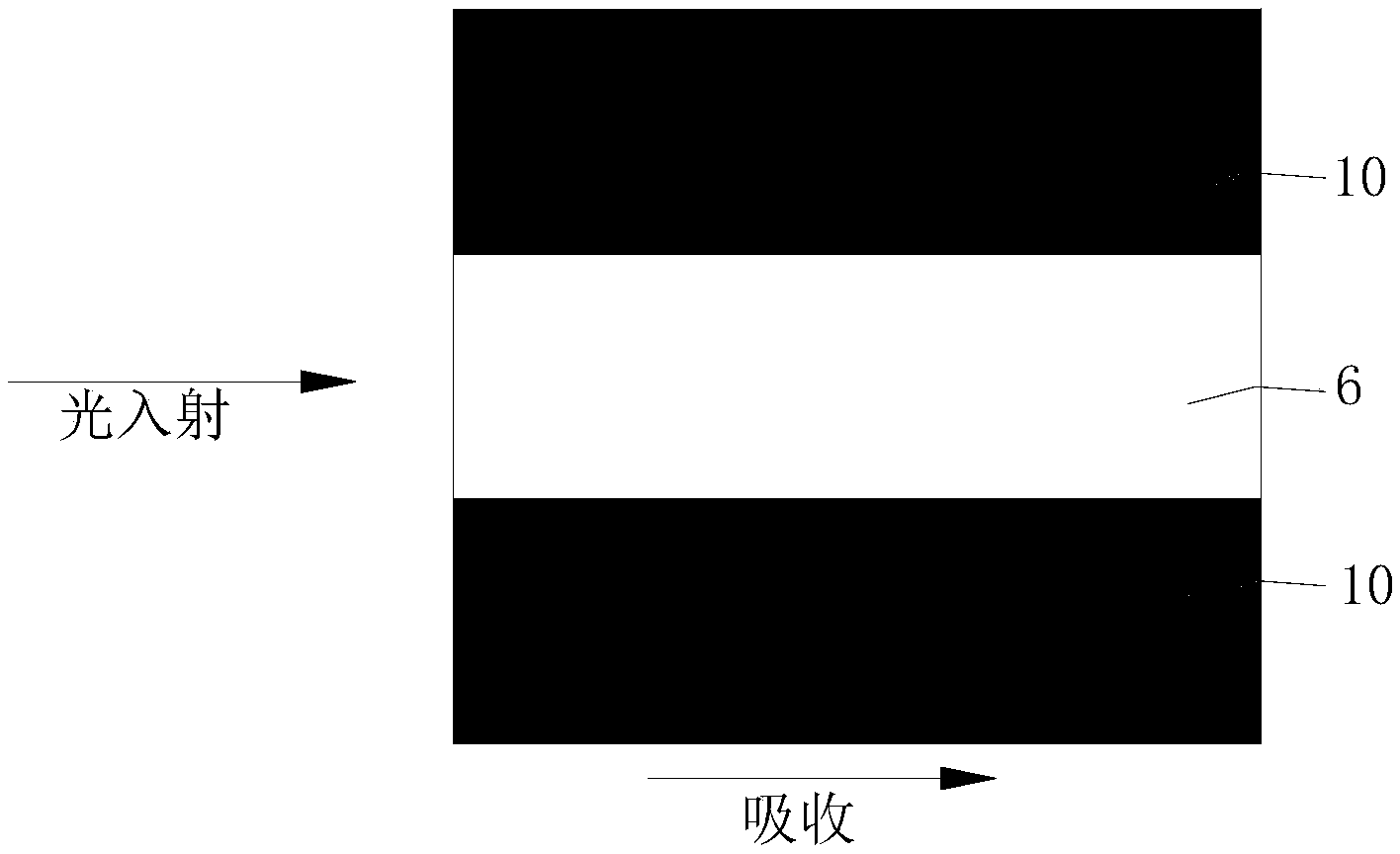
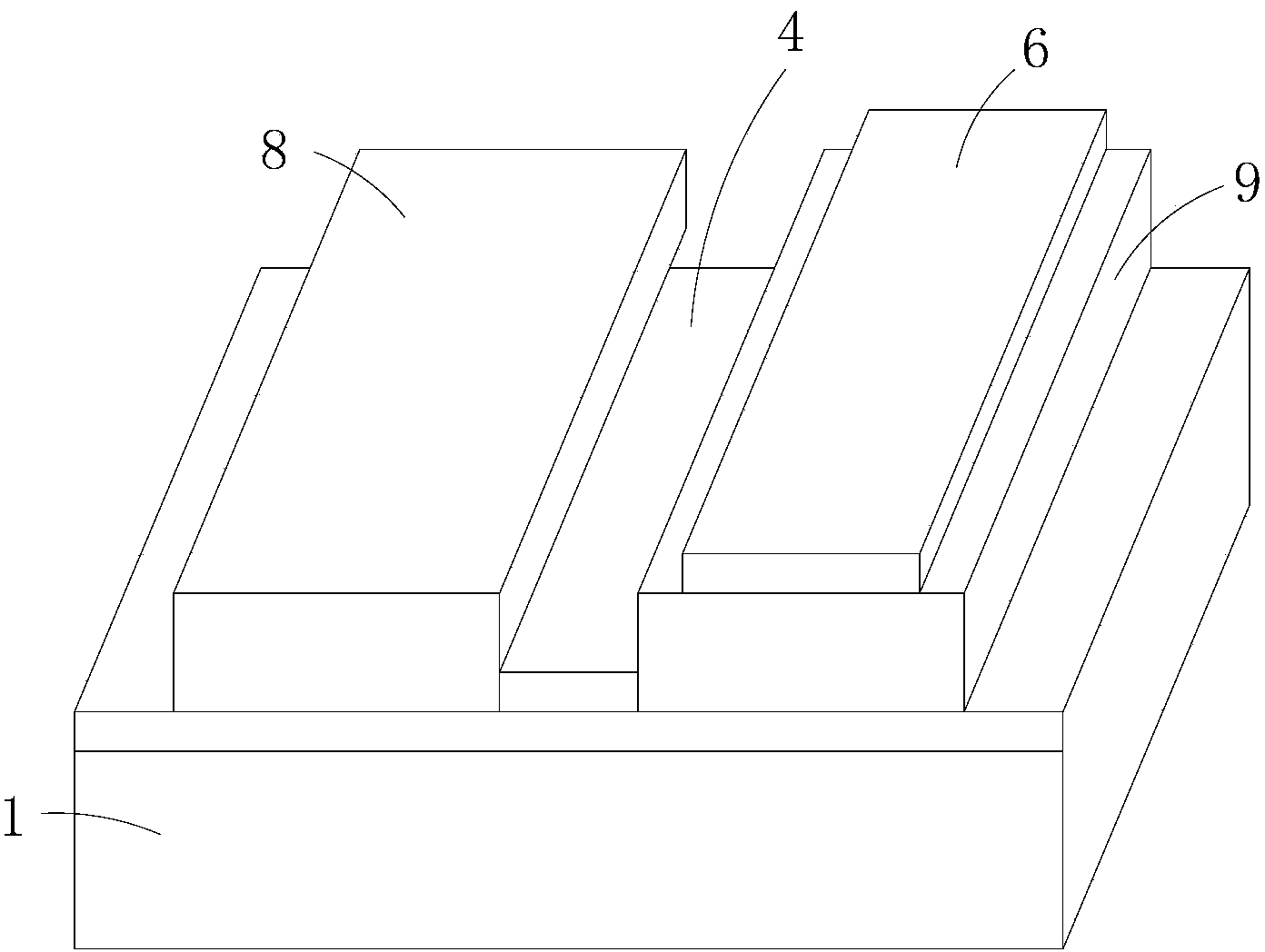
[0027] Embodiment: The following is the working wavelength of 1.55 μm, the material InGaAs (indium gallium arsenide) of the absorption layer 6, the material InGaAsP (indium gallium arsenide phosphide) of the upper waveguide layer 5, the lower waveguide layer 3 and the cover layer 2; the substrate layer 1 An example of a vertically coupled photodetector input front end of the material InP (Indium Phosphide).

[0028] First, some basic theoretical parameters of the front-end input waveguide structure of the waveguide coupler are listed:

[0029] waveguide material

Refractive index

InP

3.146

InGaAsP

3.33

InGaAs

3.56-0.1i

[0030] Table 1 Refractive index of various materials used in the detector;

[0031] Material of each layer

Thickness (μm)

Upper waveguide layer InGaAsP

3.5

Gap InP

0.09

Lower waveguide layer InGaAsP

3.05

Cladding InGaAsP

0.5

Substrate InP

15...


PUM


Abstract

The invention belongs to the field of photoelectric technology and discloses a front end input waveguide structure of a directional coupling optical waveguide detector. The front end input waveguide structure of the directional coupling optical waveguide detector comprises a substrate layer, a covering layer, a lower waveguide layer, a gap layer, an upper waveguide layer and an absorption layer which are sequentially stacked from bottom to top. The front end face of the substrate layer, the front end face of the covering layer, the front end face of the lower waveguide layer, the front end face of the gap layer and the front end face of the upper waveguide layer are flush with one another, the absorption layer is located on the upper surface of the rear of the upper waveguide layer, the gap layer is a coupling layer, and the distance from the front end face of the absorption layer to the front end face of the upper waveguide layer is twice of the coupling length. The front end input waveguide structure overcomes the defects of a waveguide detector and a horizontal direction coupling waveguide detector, light current can be effectively increased, and the problem that the front end of a waveguide is overheated and burnt because of the pattern evolution problem is solved.

Description

technical field [0001] The invention belongs to the field of optoelectronic technology, and relates to a waveguide photodiode, in particular to a front-end input waveguide structure of a directional coupling optical waveguide detector. Background technique [0002] The high-power high-speed photodetector is a detection device based on the interaction between light and matter, and its function is to convert the incident light signal into a high-power high-frequency signal. High-power high-speed optical detector is an indispensable device in optically controlled phased array radar, ultra-high-speed test system and optical fiber LAN communication, and its performance plays a decisive role in the whole system. [0003] Conventional vertical-incidence photodetectors cannot meet both high-speed and high-power requirements. The main reasons are as follows: one is the saturation effect, which limits the photocurrent; the other is the long transit time, which limits the response fre...

Claims


Application Information

Patent Timeline
IPC IPC(8): G02B6/122G02B6/24
Inventor 余学才毛康王玉杰江倩
Owner UNIV OF ELECTRONICS SCI & TECH OF CHINA
Why Eureka
Try Eureka