A method for detecting the etching ability of pattern structure

A detection method and pattern structure technology, applied in semiconductor/solid-state device testing/measurement, electrical components, semiconductor/solid-state device manufacturing, etc. question

Active Publication Date: 2017-02-22
SHANGHAI HUALI MICROELECTRONICS CORP
View PDF5 Cites 0 Cited by
  • Summary
  • Abstract
  • Description
  • Claims
  • Application Information

AI Technical Summary

Problems solved by technology

[0006] In view of the above problems, the present invention provides a method for etching ability of pattern structure, to solve the problem that the detection of etching ability and the optimal etching process window cannot be guaranteed in the prior art, and it is impossible to monitor the etching process through long-term testing. Stability and reliability defects

Method used


Image

  • A method for detecting the etching ability of pattern structure
  • A method for detecting the etching ability of pattern structure
  • A method for detecting the etching ability of pattern structure

Examples


Embodiment Construction

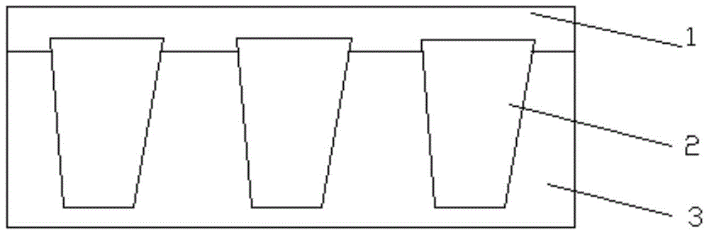
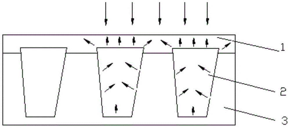
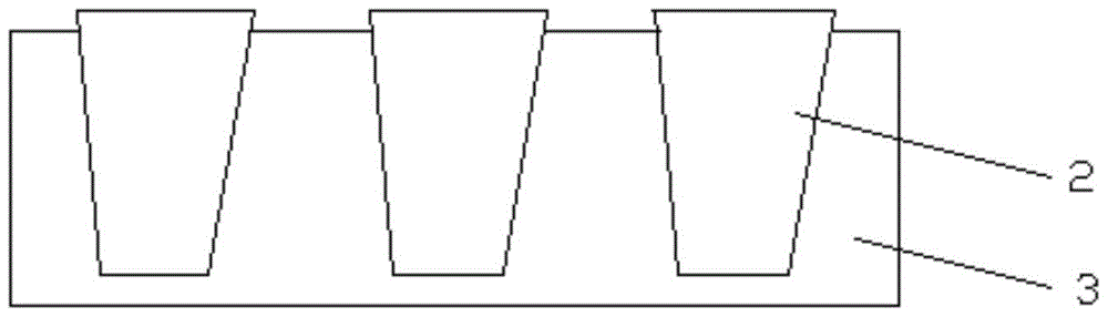
[0030] In order to improve the stability of the etching process and ensure the reliability of the etching process through long-term testing of the etching capacity, the invention provides a method for detecting the etching capacity of the pattern structure.

[0031] Specifically, such as Figures 6A-9 As shown, a semiconductor substrate including several active regions 3 and an oxide isolation layer covering the surface is provided, and an STI (Shallow Trench Isolation, shallow trench isolation) structure 2 is arranged in the active region 3, and each active region The source region 3 is surrounded and spaced apart by the STI structure 2, such as Figure 6A and Figure 6B shown. In an optional but non-limiting embodiment, a plurality of active regions 3 are arranged, arranged in a row, and used as a plurality of monitoring structures or test structures (3a 1 、3a 2 、3a 3 …3a n ), note that n is a natural number that is not zero, the test structure (3a 1 、3a 2 、3a 3 …3a...


PUM


Abstract

The invention relates to the field of circuit fault detecting techniques, in particular to a method for detecting the etching capacity of a graph structure. After a semiconductor substrate of a special structure is provided and placed on a cutting channel of a wafer, a bottom anti-reflective coating and a polycrystalline silicon layer are deposited on the upper surface of the substrate in sequence, and then the polycrystalline silicon layer and the bottom anti-reflective coating are etched by adopting photoetching and etching processes. The conditions of residues, on structures of different sizes, of the bottom anti-reflective coating are observed under an electron microscope, so that the etching capacity of the bottom anti-reflective coating with different uniformities corresponding to different sizes in an active area to graphs is analyzed, the optimum size process window suitable for being coated with the bottom anti-reflective coating and applicable to a subsequent etching process is analyzed, and the stability and reliability of process performance of the graph structure are monitored by detecting the etching capacity for a long time.

Description

technical field [0001] The invention relates to the technical field of detecting circuit defects, in particular to a method for detecting the etching ability of a graphic structure. Background technique [0002] In the existing technical field, the manufacturing process of a chip often includes hundreds of steps, and the main process modules can be divided into several parts such as photolithography, etching, ion implantation, film growth and cleaning. With the development of integrated circuit technology and the continuous reduction of feature size, the distribution of circuits on the chip is becoming more and more complex. A small error in any link will lead to the failure of the entire product, so the requirements for process control are becoming more and more stringent. In order to detect product defects in time, in the actual production process, it is necessary to carry out daily simulation monitoring of equipment process performance on the test wafer, such as etching r...

Claims


Application Information

Patent Timeline
Patent Type & Authority Patents(China)
IPC IPC(8): H01L21/66
CPCH01L21/67063H01L21/67253H01L22/12H01L22/20
Inventor 倪棋梁陈宏璘龙吟
Owner SHANGHAI HUALI MICROELECTRONICS CORP
Why Eureka
Try Eureka