Supercharge Your Innovation With Domain-Expert AI Agents!

Bus switching circuit

A bus switch and circuit technology, applied in the direction of electronic switches, logic circuit connection/interface layout, electrical components, etc.

Inactive Publication Date: 2014-12-24
KK TOSHIBA
View PDF6 Cites 2 Cited by
  • Summary
  • Abstract
  • Description
  • Claims
  • Application Information

AI Technical Summary

Problems solved by technology

However, if the pulse width of the pulse signal is shortened, the level of the output signal will drop below the specified level due to ringing caused by the influence of the load capacitance and wiring inductance.

Method used


Image

  • Bus switching circuit
  • Bus switching circuit
  • Bus switching circuit

Examples


no. 1 Embodiment approach )

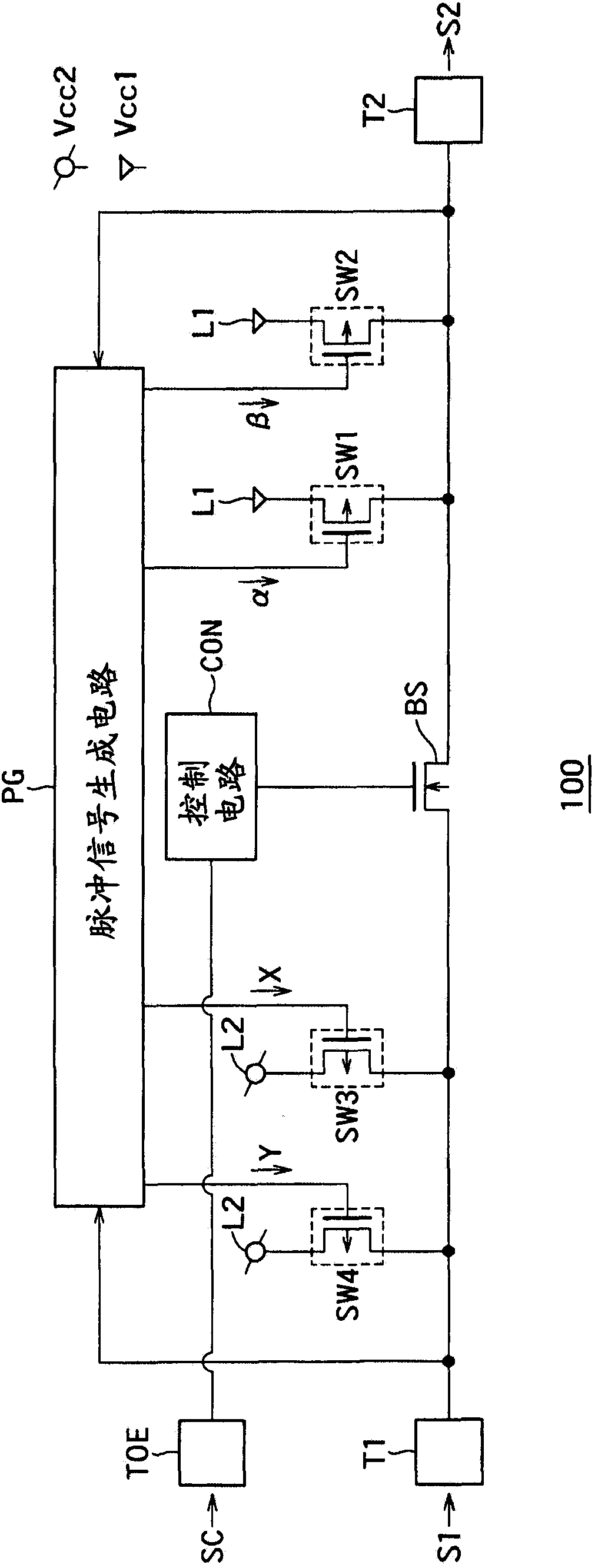
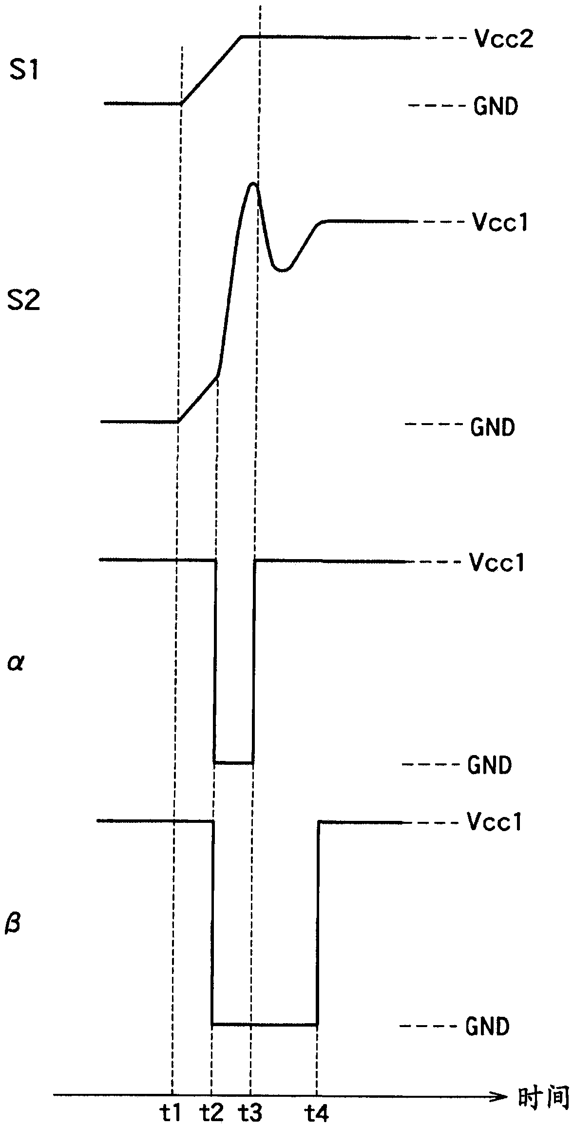
[0020] figure 1 It is a circuit diagram showing an example of the circuit configuration of the bus switch circuit 100 of the first embodiment.

[0021] like figure 1 As shown, the bus switch circuit 100 includes a control terminal TOE, a first input-output terminal T1, a second input-output terminal T2, a bus switch element BS, a first switch element SW1, a second switch element SW2, a third switch element SW3, a second switch element 4 Switching element SW4, pulse signal generating circuit (signal generating circuit) PG, control circuit CON.

[0022] The first input / output terminal T1 is connected to, for example, a first logic circuit (not shown). A signal S1 is input from the first logic circuit to the first input-output terminal T1, or a signal S1 is output from the first input-output terminal T1 to the first logic circuit. In addition, in figure 1 In the example shown, the case where the signal S1 is input to the first input-output terminal T1 from the outside is show...

no. 2 Embodiment approach )

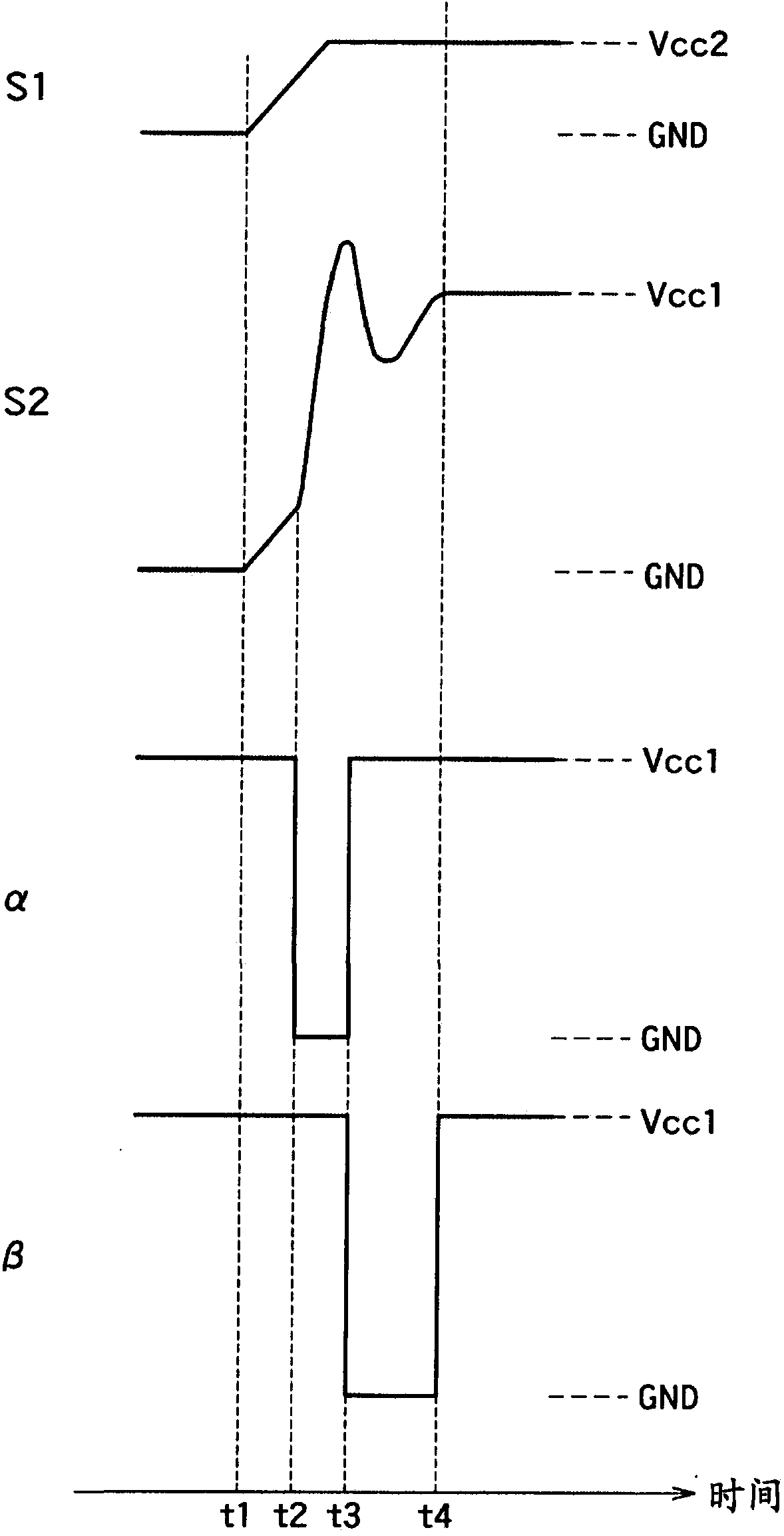
[0126] In the first embodiment described above, a configuration example of the bus switch circuit in which the first to fourth switching elements are pMOS transistors has been described. In this configuration, the rising speed of the signal is increased.

[0127] On the other hand, in this second embodiment, a configuration example of a bus switch circuit in which the first to fourth switching elements are nMOS transistors will be described. In this configuration, the speed of falling of the signal is increased.

[0128] Figure 7 It is a circuit diagram showing an example of the configuration of the bus switch circuit 200 of the second embodiment. In addition, in Figure 7 in, with figure 1 The same reference numerals represent the same configuration as that of the first embodiment.

[0129] like Figure 7 As shown, the bus switch circuit 200 includes a control terminal TOE, a first input-output terminal T1, a second input-output terminal T2, a bus switch element BS, a ...


PUM


Abstract

The invention provides a bus switching circuit capable of making an output signal level to approximate a predetermined level and transmitting a signal through a high speed. A bus switching circuit includes a bus switching element which is connected between a first input / output terminal and a second input / output terminal, a first switching element which is connected between the second input / output terminal and a first voltage wiring, and a second switching element which is connected between the second input / output terminal and the first voltage wiring, the second switching element having an internal resistance to an electric current flowing therethrough which is larger than that of the first switching element. The bus switching circuit further includes a signal generation circuit which controls the first switching element and the second switching element by outputting the first control signal and the second control signal based on a result of the comparison between a first voltage applied to the first input / output terminal and a first threshold value.

Description

[0001] Associate application [0002] This application enjoys the priority of the basic application based on Japanese Patent Application No. 2013-120071 (filing date: June 6, 2013). This application incorporates the entire content of the basic application by referring to this basic application. technical field [0003] Embodiments relate to bus switch circuits. Background technique [0004] The power supply voltage of the system LSI (Large Scale Integration: Large Scale Integration) represented by the CPU (Central Processing Unit: Central Processing Unit) and the baseband IC (Integrated Circuit: Integrated Circuit) is low in order to use the process and reduce power consumption. is developing. [0005] On the other hand, since the power supply voltages of conventionally used systems and systems processing analog signals need to maintain compatibility with conventional systems, progress in lowering the voltage has been slow. [0006] As a result, when signals are transmitt...

Claims


Application Information

Patent Timeline
IPC IPC(8): H03K19/0175
CPCH03K17/693H03K2217/0054H03K17/145
Inventor 泷场明
Owner KK TOSHIBA
Features
  • R&D
  • Intellectual Property
  • Life Sciences
  • Materials
  • Tech Scout
  • Unparalleled Data Quality
  • Higher Quality Content
  • 60% Fewer Hallucinations
Learn More