Three-dimensional circuit manufacturing method and thermosetting spraying solution

A production method and technology of three-dimensional circuits, which are applied in the fields of printed circuit manufacturing, printed circuits, coatings, etc., can solve the problems of inability to manufacture plastic parts, integrate SLS process, and cannot meet the requirements of laser surface activation, so as to reduce the cost of industrial popularization. , Not limited by shape, meet the requirements of laser activation and conductive circuit forming

Active Publication Date: 2017-12-15
SHENZHEN SUNSHINE LASER & ELECTRONICS TECH CO LTD
View PDF8 Cites 0 Cited by
  • Summary
  • Abstract
  • Description
  • Claims
  • Application Information

AI Technical Summary

Problems solved by technology

[0007] However, traditional SLS parts cannot meet the requirements of laser surface activation, and there is no laser equipment that can effectively integrate SLS technology, so it is impossible to manufacture products with circuits inside plastic parts through traditional SLS technology

Method used


Image

  • Three-dimensional circuit manufacturing method and thermosetting spraying solution

Examples


Embodiment Construction

[0029] The embodiments of the present invention will be described in detail below with reference to the drawings. It should be emphasized that the following description is only exemplary, and is not intended to limit the scope of the present invention and its application.

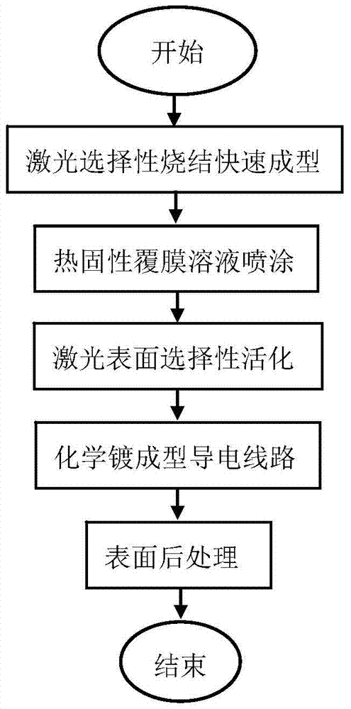
[0030] In some embodiments, a method for making a three-dimensional circuit is figure 1 As shown, the following steps are included.

[0031] step one , Generate prototype parts by selective laser sintering SLS method.

[0032] The process parameters of laser selective sintering to prepare prototype parts are as follows:

[0033] Laser selective sintering equipment is used to manufacture prototype parts. Carbon dioxide infrared laser with wavelength 10.6μm and power 10W~40W can be used as sintering source, laser scanning rate is 3~5m / s, spot diameter is 0.5mm, X, Y, Z axis processing The shrinkage compensation rate X is 2.85~3.82%, Y is 2.85~3.82%, Z(0) is 2.10~3.22%, Z(300) is 1.47~2.44%, where Z(0) refers to the...


PUM

PropertyMeasurementUnit
thicknessaaaaaaaaaa

Abstract

The invention discloses a three-dimensional circuit manufacturing method. The method comprises the steps that a prototype model is generated through a selective laser sintering method; spraying treatment and curing are carried out on the surface of the prototype model through a thermosetting spraying solution containing a soluble metal complex, and a coating film with the surface capable of being activated by laser is formed; the laser is used for carrying out preset selective scanning on the coating film to form a surface activation area; a conductive circuit is formed on the surface activation area through chemical plating. On the basis that the prototype model is obtained through the selective laser sintering method, the surface of the prototype model is coated with the coating film through the thermosetting solution, the limitation brought by traditional SLS processing materials on the application is overcome, a matrix with the complex surface is formed with no appearance limitation, and the requirements for rapid manufacturing and forming of the conductive circuit and laser activation are effectively met.

Description

Technical field [0001] The invention relates to a method for manufacturing a three-dimensional circuit and a thermosetting spray solution. Background technique [0002] For the manufacturing process and corresponding material technology of electronic appliances and electromechanical products, the pursuit of the direction is flexibility, environmental protection, speed, and energy saving. The industry has developed a technology called 3D-MID (Three-dimensional moulded interconnect deviceor electronic assemblies). This technology forms precise and compact conductive patterns on the plastic surface. Electronic components can be directly welded to the plastic shell or inner shell to form a Electronic appliances and mechatronics products for printed circuit boards. This technology is applied to the production of three-dimensional circuits, saving circuit space for electronic and electrical products and electromechanical products, and realizing flexible circuit manufacturing. Its mai...

Claims


Application Information

Patent Timeline
Patent Type & Authority Patents(China)
IPC IPC(8): H05K3/00H05K3/10C09D201/00C09D161/20C09D7/12
Inventor 蔡志祥王浩杨伟邹凯南威
Owner SHENZHEN SUNSHINE LASER & ELECTRONICS TECH CO LTD
Why Eureka
Try Eureka