Lead frame structure with staggered pins and semiconductor device manufacturing method

A lead frame and semiconductor technology, applied in the fields of semiconductor/solid-state device manufacturing, semiconductor devices, semiconductor/solid-state device components, etc., can solve problems such as difficulty in parallel online testing, waste of lead frame materials, and impact on work efficiency. The effect of parallel electrical performance test

Active Publication Date: 2018-04-03
SHENZHEN STS MICROELECTRONICS CO LTD
View PDF5 Cites 0 Cited by
  • Summary
  • Abstract
  • Description
  • Claims
  • Application Information

AI Technical Summary

Problems solved by technology

This leads directly to waste of lead frame material
[0007] (2) For the process based on the whole frame as the smallest operation unit (such as mold sealing, etc.), since the number of effective products at one time is only 120, this greatly affects the work of the corresponding station efficiency
[0008] (3) Since the chip stage and the pins are connected together before final molding and separation, it is difficult to implement frame-based parallel online testing

Method used


Image

  • Lead frame structure with staggered pins and semiconductor device manufacturing method
  • Lead frame structure with staggered pins and semiconductor device manufacturing method
  • Lead frame structure with staggered pins and semiconductor device manufacturing method

Examples


no. 1 example

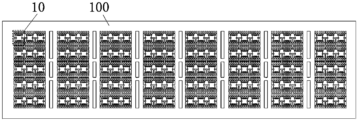
[0065] Figure 4 According to a specific embodiment of the present invention, a partial structural schematic diagram of the base material of the lead frame adopting the staggered pins of the present invention is shown. Such as Figure 4 As shown, the lead frame structure with staggered pins of the present invention is formed on a substrate 100 and includes: a plurality of chip units 20 arranged in a matrix. Twelve chip units 20 are arranged in each column, but not limited thereto. Compared with the 5x3x8 array lead frame in the prior art, in order to minimize the width of the monolithic frame, the present invention introduces the staggered pin form into the frame design.

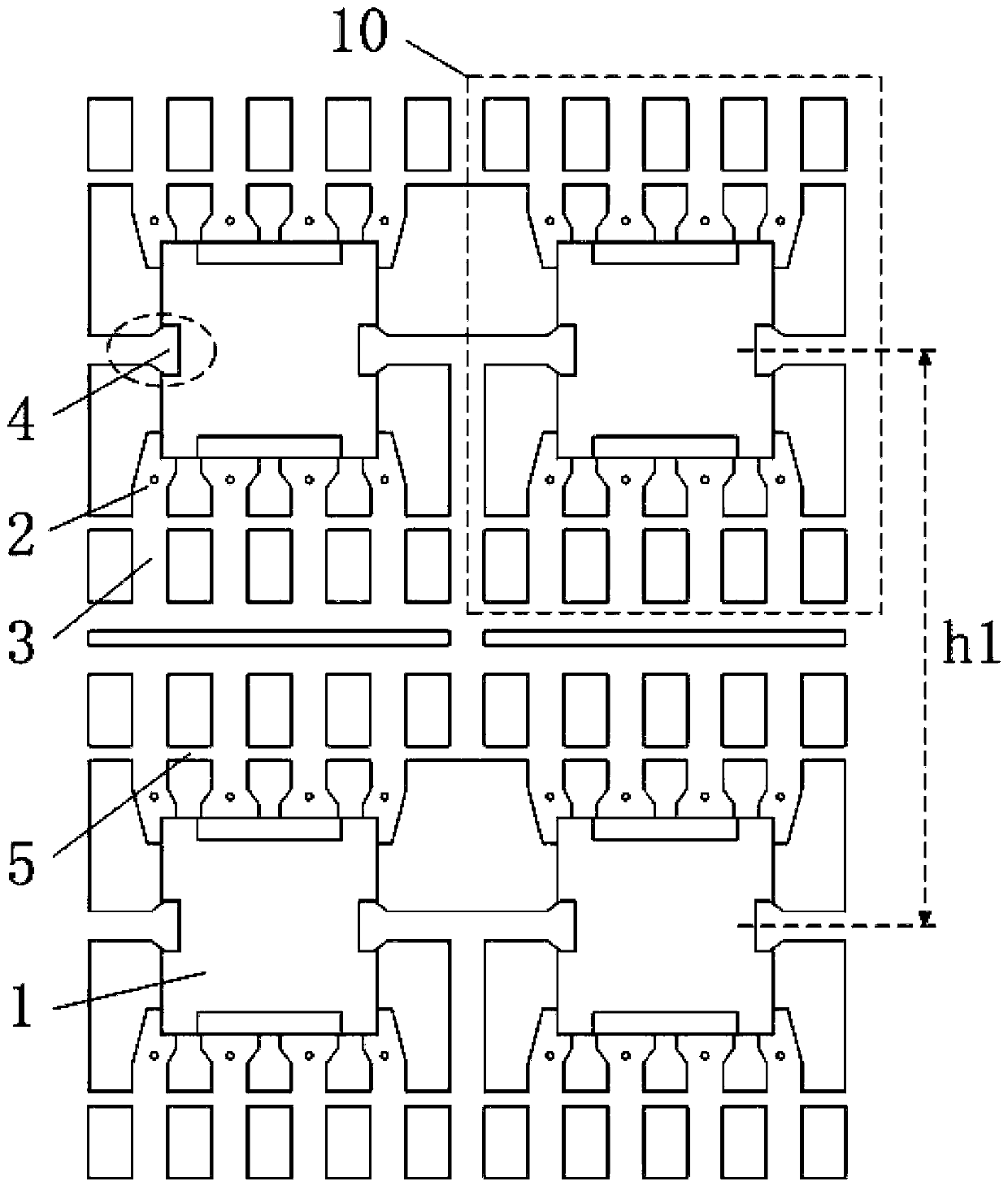
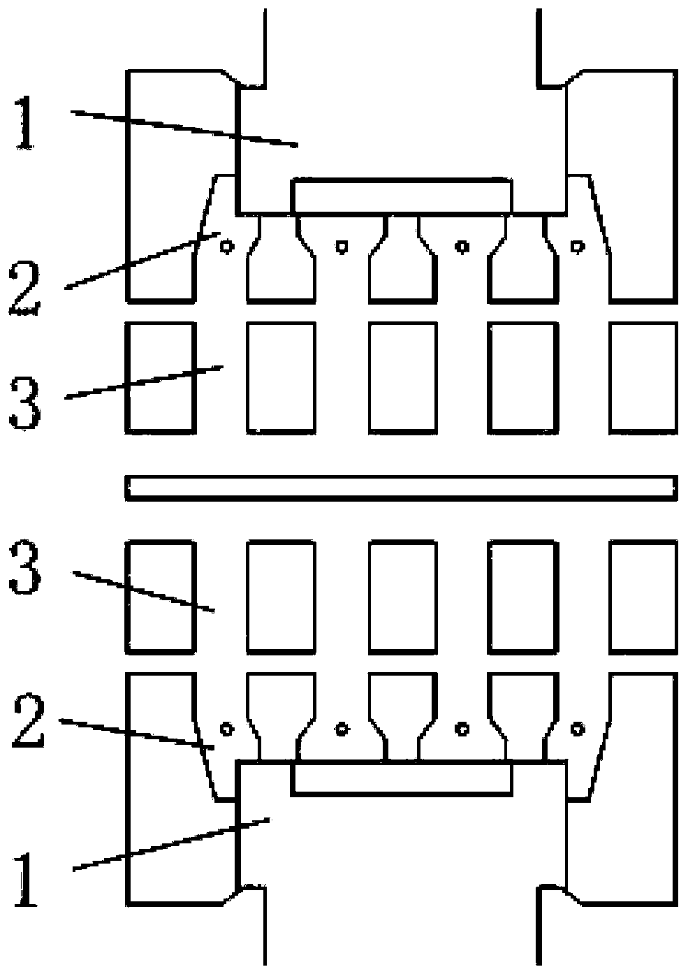
[0066] Figure 5 A schematic diagram showing a lead frame structure with staggered pins according to a specific embodiment of the present invention. Such as Figure 5As shown, each chip unit 20 includes at least one chip stage 11 , a plurality of outer pins 13 are drawn out from the periphery of the chi...


PUM


Abstract

The invention provides a base-pin-staggering-mode-based lead frame structure and a semiconductor device manufacturing method. The lead frame structure formed on a substrate comprises a plurality of chip units; each chip unit includes at least one chip bench; a plurality of outer base pins are led out outwardly from a plurality of inner lead pins around each chip bench; and outer base pin regions of the adjacent chip benches are overlapped. In addition, the semiconductor device manufacturing method comprises: a silicon wafer is bonded to the chip benches of the base-pin-staggering-mode-based lead frame structure; all welding plates of the silicon wafer are coupled with the inner lead pins in the lead frames; resin molding is carried out; aging is carried out in a high-temperature environment; overflow connecting ribs are cut off; parallel testing is carried out; and cutting is carried out to form a semiconductor device. According to the invention, the staggered pin mode is introduced into the frame design; and the space occupied by the outer base pins between the two parallel chip benches can be reduced, so that the outer base pin regions of the two parallel chip benches are overlapped. Moreover, the outer frame connecting ribs are arranged and parallel electric performance testing can be realized.

Description

technical field [0001] The invention relates to a lead frame structure, in particular to a lead frame structure with staggered pins that rationally uses the area of ​​the base material and improves the ratio of the effective chip area to the entire lead frame, and a semiconductor device manufacturing method using the structure. Background technique [0002] In the process of chip fabrication, traditional chip packaging forms a plurality of chip units 10 arranged in matrix on the substrate 100 . The following is an example of a chip package arranged in an array: figure 1 A schematic diagram showing a substrate of a prior art chip package. Such as figure 1 As shown, a traditional chip package adopts a 5x3x8 array, and a total of 120 chip units 10 are formed on a substrate 100, that is, a lead frame of 120 products is integrated on a substrate of 57mmx215.7mm. [0003] figure 2 A schematic diagram showing the structure of a chip unit in a substrate of a chip package in the...

Claims


Application Information

Patent Timeline
Patent Type & Authority Patents(China)
IPC IPC(8): H01L23/495H01L21/50
CPCH01L2224/97
Inventor 匡秋虹张萍曾宪洪王燕包杰管杰骏
Owner SHENZHEN STS MICROELECTRONICS CO LTD
Why Eureka
Try Eureka