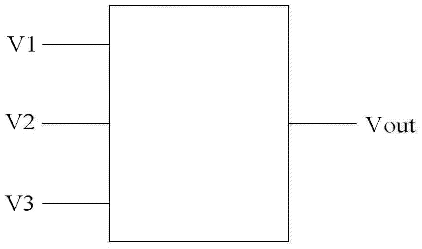
Three-input general logic gate circuit
A logic gate circuit and three-input technology, applied to logic circuits with logic functions, etc., can solve the problems of slow switching speed, high power consumption, and large volume, and achieve the effect of high switching speed and low power consumption
- Summary
- Abstract
- Description
- Claims
- Application Information
AI Technical Summary
Problems solved by technology
Method used
Image

Examples
Embodiment Construction
[0020] The present invention will be further described below in conjunction with the drawings.
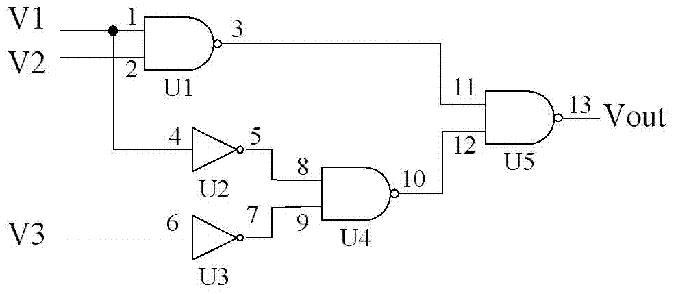
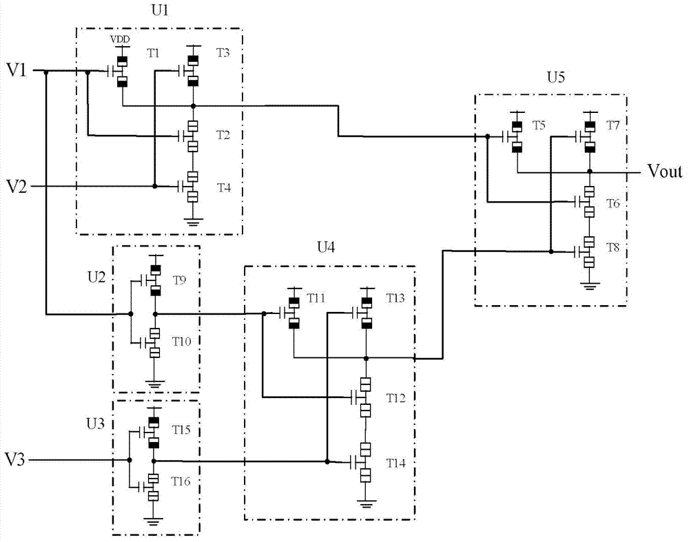
[0021] Reference Figure 1 ~ Figure 5 , A three-input general logic gate circuit, the circuit includes a first two-input NAND gate U1, a second two-input NAND gate U4, a third two-input NAND gate U5, a first two-input NAND gate U2 and a second inverter Gate U3, the first two-input NAND gate U1, the second two-input NAND gate U4, the third two-input NAND gate U5, the first inverter U2, and the second inverter U3 are all composed of single-electron transistors;
[0022] The first input terminal of the first two-input NAND gate U1 is connected to the input terminal of the first NOT gate U2 as the first input terminal V1 of the general logic gate circuit, and the second input terminal of the first two-input NAND gate U1 is used as The second input terminal V2 of the universal logic gate circuit, the output terminal of the first two-input NAND gate U1 and the first input terminal of the thi...
PUM
 Abstract
Description
Claims
Application Information
 - R&D
- Intellectual Property
- Life Sciences
- Materials
- Tech Scout
- Unparalleled Data Quality
- Higher Quality Content
- 60% Fewer Hallucinations
Browse by: Latest US Patents, China's latest patents, Technical Efficacy Thesaurus, Application Domain, Technology Topic, Popular Technical Reports.
© 2025 PatSnap. All rights reserved.Legal|Privacy policy|Modern Slavery Act Transparency Statement|Sitemap|About US| Contact US: help@patsnap.com