Multi-PDN type current mode RM logic circuit

A logic circuit and current mode technology, applied to logic circuits with logic functions, etc., can solve the problems of no RM logic compound gate logic unit, no power consumption optimization RM logic standard unit, etc., to achieve good power consumption effect, low Effects of Power Consumption, Latency, and Power Delay Product Reduction

Active Publication Date: 2015-01-07
SHANDONG LANDBRIDGE PETROCHEMICAL CO LTD
View PDF4 Cites 4 Cited by
  • Summary
  • Abstract
  • Description
  • Claims
  • Application Information

AI Technical Summary

Problems solved by technology

Today's integrated circuit design relies more on the design of logic cell libraries. However, traditional logic cell libraries are designed for the synthesis and optimization of TB logic, and do not include RM logic standard cells that have been optimized for power consumption, let alone RM Logic Composite Gate Logic Unit

Method used


Image

  • Multi-PDN type current mode RM logic circuit
  • Multi-PDN type current mode RM logic circuit
  • Multi-PDN type current mode RM logic circuit

Examples


Embodiment 1

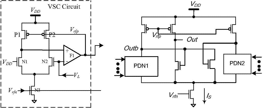
[0028] Embodiment one: if figure 1 with figure 2 As shown, a multi-PDN type current mode RM logic circuit includes a voltage swing control circuit VSC and a composite gate logic circuit, and the voltage swing control circuit VSC includes a first PMOS transistor P1, a second PMOS transistor P2, a first NMOS transistor N1, the second NMOS transistor N2, the third NMOS transistor N3 and the first operational amplifier F1, the source of the first PMOS transistor P1, the substrate of the first PMOS transistor P1, the source of the second PMOS transistor P2, the second PMOS The substrate of the transistor P2 and the gate of the first NMOS transistor N1 are connected to the power supply V DD connected, the substrate of the first NMOS transistor N1, the substrate of the second NMOS transistor N2, the substrate of the third NMOS transistor N3 and the source of the third NMOS transistor N3 are all connected to the ground V SS The drain of the first PMOS transistor P1, the drain of th...

Embodiment 2

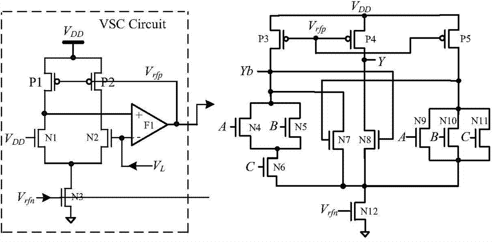
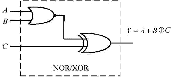
[0049] Embodiment 2: The circuit structure of this embodiment is exactly the same as that of Embodiment 1. By changing the first input logic signal, the second input logic signal and the third input logic signal in the input RM circuit, the following can be obtained: Figure 4 The composite gate composed of the NAND gate and the XOR gate is shown, and its symbol diagram is as follows Figure 5 shown.

[0050] In this embodiment, the first input logic signal connected to the first signal input end of the RM logic circuit is Ab, the second input logic signal connected to the second signal input end of the RM logic circuit is Bb, and the second input logic signal of the RM logic circuit is Bb. The third input logic signal connected to the three-signal input terminal is Cb, wherein, is the inversion signal of A, is the inverse signal of B, Inverted signal for C.

[0051] Analyze the RM logic circuit of the present embodiment, can obtain:

[0052] PDN ...


PUM


Abstract

The invention discloses a multi-PDN type current mode RM logic circuit. A voltage swing control circuit and a compound logic gate circuit form the RM logic circuit which is a current mode circuit virtually. A fourth NMOS tube, a fifth NMOS tube and a sixth NMOS tube in the compound logic gate circuit form a first pull-down network (PDN), a ninth NMOS tube, a tenth NMOS tube and an eleventh NMOS tube in the compound logic gate circuit form a second pull-down network (PDN), and the multi-PDN type structure is suitable for achieving complex logic functions and accordingly achieving the functions of the current mode compound logic gate circuit formed by multiple logic gates. The RM logic circuit has the advantage that under the condition that circuit functions are not influenced, the power consumption of the circuit can be effectively reduced by adopting the current mode technology. Compared with an existing current mode RM logic circuit and a traditional RM logic circuit, the power consumption, the time delay and the power consumption-time delay product of the RM logic circuit are substantially reduced. As is verified by experimentation, the RM logic circuit has the excellent effect of low power consumption under the SMIC130 nm process.

Description

technical field [0001] The invention relates to an RM logic circuit, in particular to a multi-PDN current mode RM logic circuit. Background technique [0002] Digital circuits can be implemented based on traditional Boolean logic (TB), or Reed-Muller (RM) logic based on operation sets such as "or / exclusive or" and "and / exclusive or". Studies have shown that RM logic circuits have more advantages than TB logic circuits in terms of implementation cost, system testability, and circuit performance improvement (such as area, speed, power consumption, etc.). With the advancement of integrated circuit technology, more and more attention has been paid to the research on RM logic, and many research results have been achieved, such as logic functions based on AND / OR operators and logic based on AND / XOR operators. Transformation between functions, RM expansion of logic functions, polarity optimization of RM functions, logic synthesis theory of RM functions, etc. However, most of thes...

Claims


Application Information

Patent Timeline
Patent Type & Authority Applications(China)
IPC IPC(8): H03K19/20
Inventor 胡建平韩承浩
Owner SHANDONG LANDBRIDGE PETROCHEMICAL CO LTD
Why Eureka
Try Eureka