Polycrystalline silicon manufacturing method

A production method and technology of polysilicon, applied in the direction of manufacturing tools, semiconductor/solid-state device manufacturing, laser welding equipment, etc., can solve problems such as the inability of the amorphous silicon layer to reach the melting temperature, high excimer laser energy, and unstable crystallization rate of polysilicon , to achieve the effects of reducing the number of launches, reducing costs, and reducing temperature gradients

Inactive Publication Date: 2015-01-14
EVERDISPLAY OPTRONICS (SHANGHAI) CO LTD
View PDF5 Cites 4 Cited by
  • Summary
  • Abstract
  • Description
  • Claims
  • Application Information

AI Technical Summary

Problems solved by technology

[0004] However, in the existing polysilicon production method using excimer laser annealing, the laser energy cannot quickly bring the amorphous silicon layer to the melting temperature, but needs to use multiple pulses of excimer laser energy to make the amorphous silicon lay

Method used


Image

  • Polycrystalline silicon manufacturing method
  • Polycrystalline silicon manufacturing method
  • Polycrystalline silicon manufacturing method

Examples


Embodiment Construction

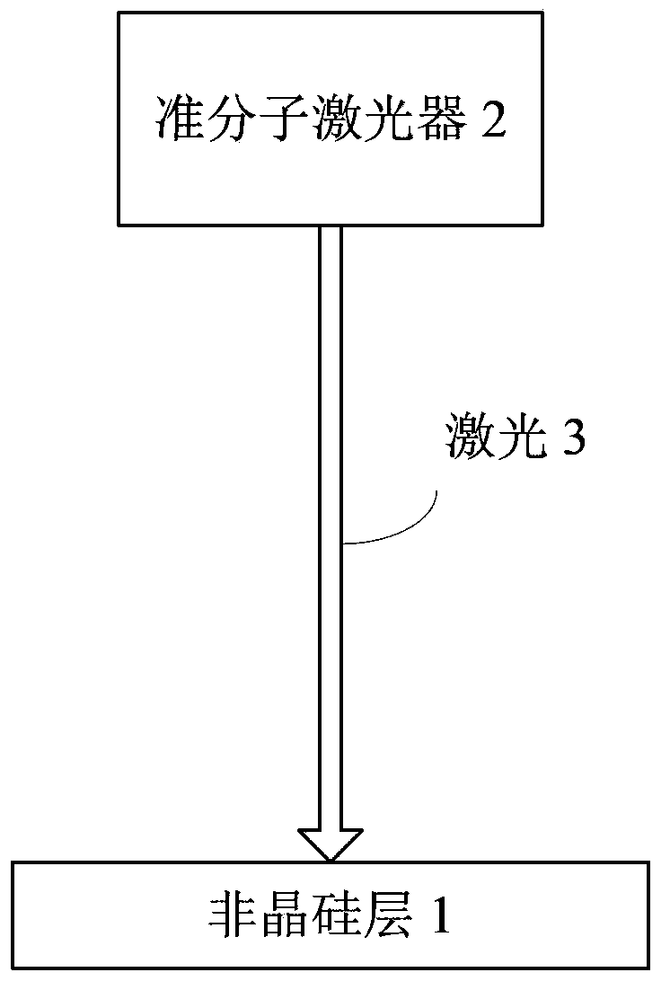
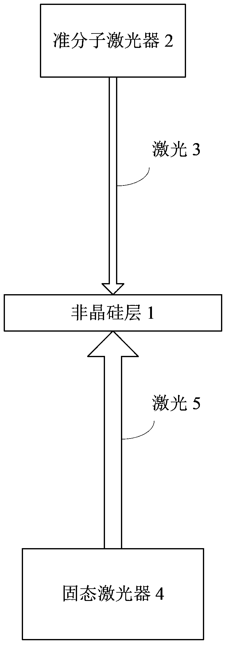
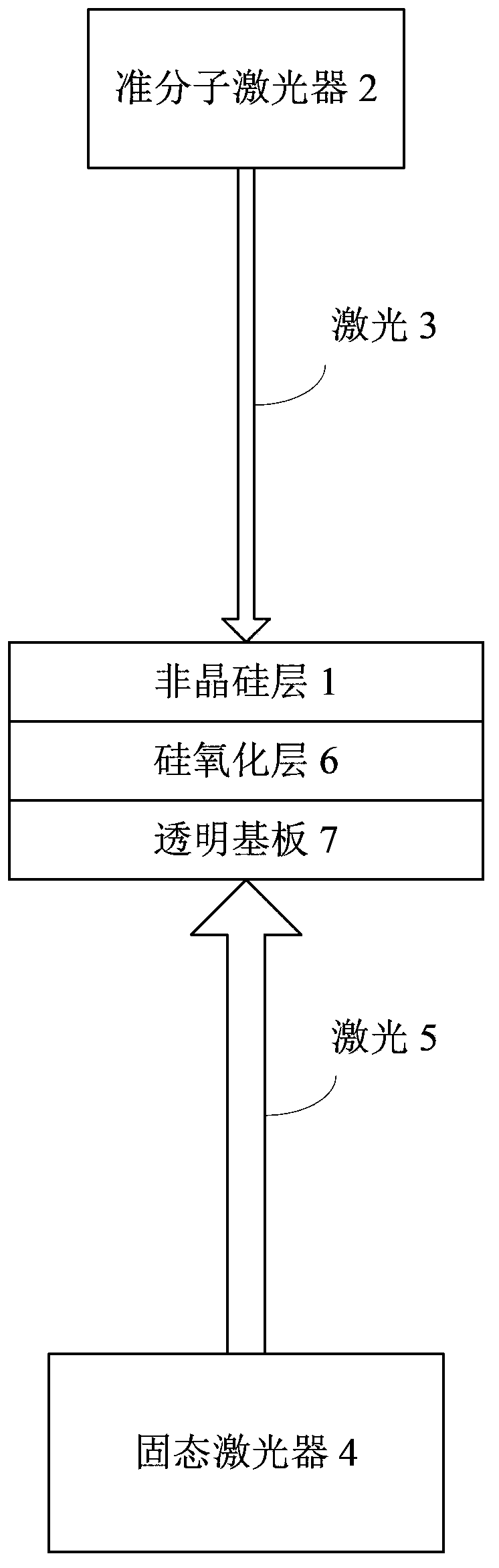
[0025] The following will combine Figure 2 to Figure 6 The present application is described in detail, wherein the same reference numerals represent the same or similar devices, substances or steps.

[0026] figure 2 A schematic diagram illustrating a method for fabricating polysilicon using excimer laser annealing according to the first embodiment of the present application is exemplarily shown. Such as figure 2 as shown in the figure 1 The polysilicon manufacturing method that adopts excimer laser annealing in the prior art shown in is different, and the present application except using excimer laser 2 to emit laser light 3 to irradiate the upper surface of amorphous silicon layer 1, also uses solid-state laser 4 to emit The laser 5 is used to irradiate the lower surface of the amorphous silicon layer 1 to preheat or assist the heating of the amorphous silicon layer 1, thereby facilitating the melting of the amorphous silicon layer 1 and crystallization into polysilico...


PUM

PropertyMeasurementUnit
Wavelengthaaaaaaaaaa

Abstract

A polycrystalline silicon manufacturing method comprises the steps that S11 a solid-state laser device is used for emitting lasers to irradiate the lower surface of a non-crystalline silicon layer so as to preheat the non-crystalline silicon layer; S12 a quasimolecule laser device is used for irradiating the upper surface of the non-crystalline silicon layer so as to crystallize the non-crystalline silicon layer to form polycrystalline silicon, wherein the step S11 is executed earlier than the step S12 by preset time or simultaneously with the step S12. The polycrystalline silicon manufacturing method can greatly shorten the time for melting and crystallizing the non-crystalline silicon to form the polycrystalline silicon, and therefore the yield of the polycrystalline silicon is effectively increased; due to the fact that the temperature gradient during melting and crystallizing of the non-crystalline silicon is reduced, the crystallization rate of the polycrystalline silicon can be increased, and the crystallization quality of the polycrystalline silicon can be effectively improved; in addition, the emitting frequency of the expensive quasimolecule laser device can be reduced, the service life of the quasimolecule laser device is prolonged accordingly, and the cost is further reduced.

Description

technical field [0001] The present application relates to a polysilicon manufacturing method, in particular to a polysilicon manufacturing method using excimer laser annealing. Background technique [0002] With the wide application of semiconductor technology, the demand for polysilicon is increasing. At present, excimer laser annealing technology has been used to produce polysilicon. [0003] figure 1 A schematic diagram of a polysilicon manufacturing method using excimer laser annealing in the prior art is exemplarily shown. Such as figure 1 As shown in, in the polysilicon manufacturing method that adopts excimer laser annealing in the prior art, excimer laser 2 emits laser light 3 and irradiates the upper surface of amorphous silicon layer 1, makes the upper surface of amorphous silicon layer 1 melt, thereby crystallized into polysilicon. For example, U.S. Patent Application No. 5,529,951 has adopted this method. It uses an excimer (excimer) laser with a wavelength ...

Claims


Application Information

Patent Timeline
IPC IPC(8): H01L21/268B23K26/00B23K26/06
CPCH01L21/02532H01L21/02595H01L21/268
Inventor 叶昱均黄德伦黄政仕
Owner EVERDISPLAY OPTRONICS (SHANGHAI) CO LTD
Why Eureka
Try Eureka