
Infrared emitter and NDIR sensor

An infrared detector and infrared technology, applied in instruments, scientific instruments, transmittance measurement, etc., can solve the problems of small infrared radiation propagation distance and low sensor sensitivity

Active Publication Date: 2015-01-14
希奥检测有限公司
View PDF22 Cites 22 Cited by
  • Summary
  • Abstract
  • Description
  • Claims
  • Application Information

AI Technical Summary

Problems solved by technology

However, in this case, since the optical path is on the chip, the infrared radiation propagation distance is very small, therefore, the sensor has low sensitivity

Method used


Image

  • Infrared emitter and NDIR sensor
  • Infrared emitter and NDIR sensor
  • Infrared emitter and NDIR sensor

Examples


Embodiment Construction

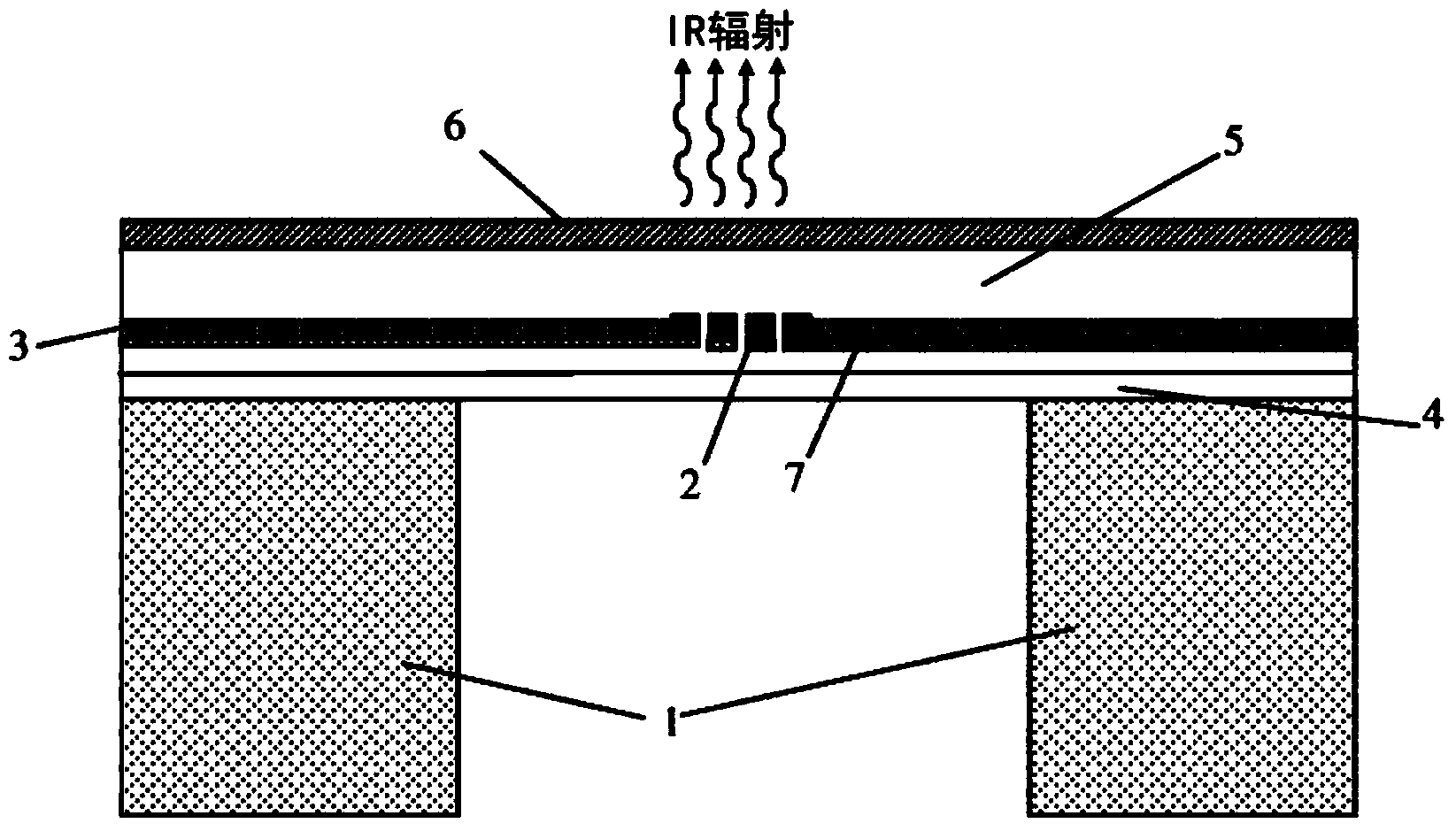
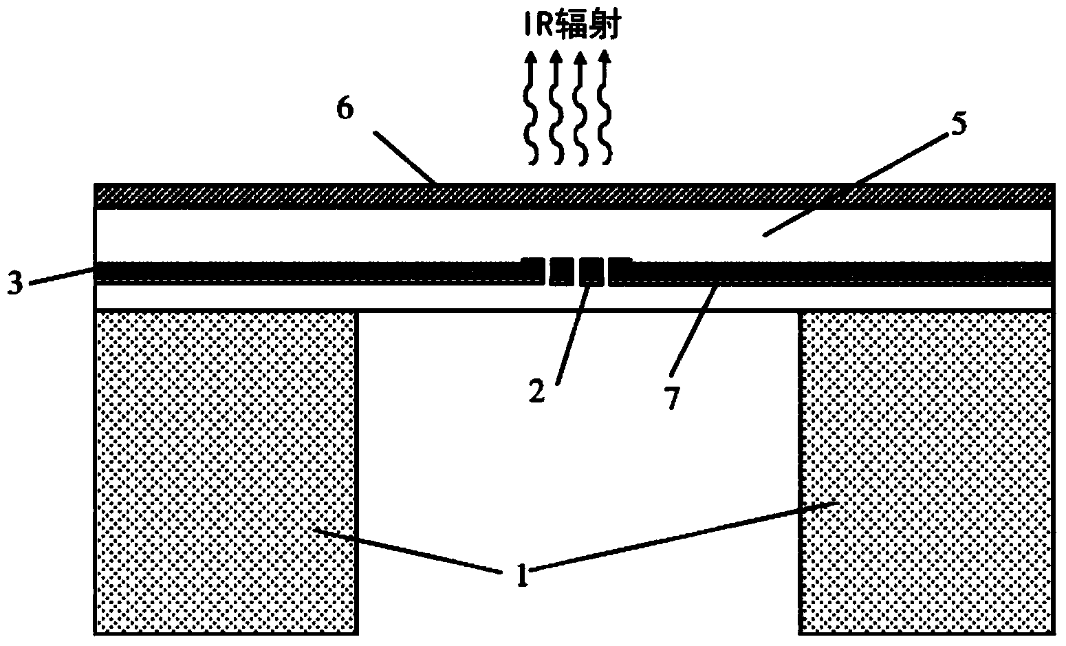
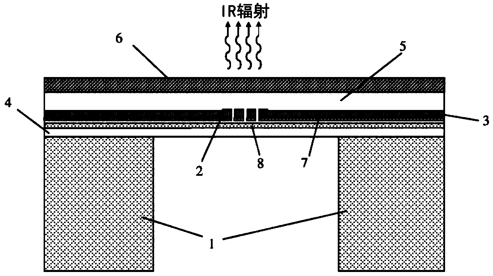
[0058] Embodiments of the present invention seek to facilitate the development of devices in this field by using CMOS layers with tungsten as part of heaters emitting infrared radiation and as interconnect metals for electronic devices. Infrared emitters are embedded in an electrolyte membrane formed by etching a silicon substrate. Etching can be accomplished by deep reactive ion etching (DRIE) techniques. Due to the use of tungsten heaters, this device is capable of reliable operation at high temperatures (well above 600°C). Furthermore, in the CMOS process, the use of tungsten layers ensures high stability, long-term reliability and high reproducibility. CMOS is very different from heaters fabricated by other techniques such as screen printing. To further increase reliability, the tungsten heater can have a titanium / titanium nitride liner. In addition, using CMOS technology to fabricate devices results in lower manufacturing costs and allows circuits to be integrated on t...


PUM


Abstract

An IR source is provided in the form of a micro-hotplate device comprising a CMOS metal layer made of at least one layer of embedded on a dielectric membrane supported by a silicon substrate. The device is formed in a CMOS process followed by a back etching step. The device is advantageous over state of the art devices as it provides a micromachined IR source capable of achieving high temperatures (and thus higher emissions), while at the same time can be fabricated by commercial CMOS processes - thus having low fabrication cost, high reproducibility and reliability and offering the possibility of monolithic integrated circuitry. The device can also be integrated with an IR detector on the same chip and packaged to form a complete NDIR sensor.

Description

technical field [0001] The present invention relates to a thermal infrared (IR) source using a microhotplate fabricated on a microchip. The invention also relates to the integration of an infrared source and an infrared detector to form an NDIR sensor. Background technique [0002] It is known to fabricate thermally effective infrared sources on silicon substrates comprising microheaters formed inside a thin film layer (consisting of an electrically insulating layer) formed by etching part of the substrate. Such devices can be used to provide heat (eg, 600° C.) at low power consumption (typically from a few milliwatts to hundreds of milliwatts) for use as an infrared source / emitter. [0003] For example, "Micro-machined thermal emitter from a commercial CMOS process," by Parameswaran et al., reported in IEEE EDL 1991 that a polysilicon heater for IR applications manufactured with CMOS technology uses front etching to suspend the heater, thereby reducing work consumption. ...

Claims


Application Information

Patent Timeline
IPC IPC(8): H05B3/14G01N27/16G01N21/35H05B3/26
CPCH05B2203/032H05B2203/017H05B3/143G01N21/61H05B3/267G01N21/3504H05B3/0047
Inventor S·Z·阿里F·乌德雷亚J·加德纳M·F·乔杜里I·波埃纳鲁
Owner 希奥检测有限公司
Features
  • Generate Ideas
  • Intellectual Property
  • Life Sciences
  • Materials
  • Tech Scout
  • Unparalleled Data Quality
  • Higher Quality Content
  • 60% Fewer Hallucinations
Learn More