Device and method for measuring smooth free-form surface sample based on differential STED

A sample, free technology, applied in measurement devices, optical devices, instruments, etc., can solve the problems of inability to overcome the extremely weak light intensity of collected signals and no industrial samples yet.

Active Publication Date: 2015-01-21
HARBIN INST OF TECH
View PDF13 Cites 16 Cited by
  • Summary
  • Abstract
  • Description
  • Claims
  • Application Information

AI Technical Summary

Problems solved by technology

Since the measurement objects in the field of industrial measurement cannot emit fluorescence, STED microscopy devices are mainly used in the field of biological microscopic imaging, and there is no precedent for application in the shape measurement of industrial samples.
Even if STED microscopy is simply transplanted to the field of industrial sample shape measurement, it cannot overcome the problem that the light intensity of the collected signal is extremely weak due to the specular reflection of the beam on the sample surface with a smooth free-form surface

Method used


Image

  • Device and method for measuring smooth free-form surface sample based on differential STED
  • Device and method for measuring smooth free-form surface sample based on differential STED
  • Device and method for measuring smooth free-form surface sample based on differential STED

Examples


specific Embodiment 1

[0039] This embodiment is a device embodiment.

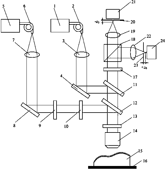
[0040] The device for measuring smooth free-form surface samples based on differential STED in this embodiment, the structural diagram is as follows figure 1 shown. The device includes: an excitation module, a loss module, a differential imaging module and a coated sample 15;

[0041] The excitation module includes: a wavelength of λ 1 The first picosecond pulse laser 1, the first guiding fiber 2, the first collimating objective lens 3, and the first plane mirror 4;

[0042] The loss module includes: the wavelength is λ 2 The second picosecond pulse laser 5, the second guide fiber 6, the second collimating objective lens 7, the second plane mirror 8, the vortex phase modulation plate 9 and the half-wave plate 10;

[0043] The differential imaging module includes: a first dichroic mirror 11, a second dichroic mirror 12, a quarter wave plate 13, a focusing objective lens 14, a three-dimensional micro-displacement stage 16, an ...


PUM


Abstract

The invention provides a device and method for measuring a smooth free-form surface sample based on differential STED, and belongs to the field of optical microscopic measurement. The surface of the smooth free-form surface sample is plated with a fluorescent film, and by the utilization of the characteristic that the fluorescent film radiates fluorescence in various directions under laser radiation, the problem that signal light is difficult to collect due to specular reflection of light beams on a smooth free-form surface is solved; meanwhile, by the adoption of the STED microscopy principle, light spots formed by collecting two pulse laser beams of different wavelengths coincide with each other, the portions, located in the center regions of the light spots, of the fluorescent film on the sample excite fluorescence, the portions, located in the light spots but not located in the center regions of the light spots, of the fluorescent film generate back excitation and do not emit fluorescence, and therefore super-resolution imaging of the sample is achieved; by the adoption of a differential detection structure, differential operation is conducted on two paths of collected signals, a differential response curve is acquired, the surface position of the sample is determined through a zero point of the differential response curve, and finally the purpose of measuring the smooth free-form surface sample shape with the large curvature at high accuracy is achieved.

Description

technical field [0001] A device and method for measuring smooth free-form surface samples based on differential STED belongs to the field of optical microscopic measurement. Background technique [0002] For samples with a smooth free-form surface, in the area where the angle between the normal line and the optical axis direction is large, the light illuminating the sample surface cannot be completely collected due to specular reflection, or can hardly be collected, so the surface topography cannot be highly accurate. Measure, not even measure. Therefore, how to measure a sample with a smooth free-form surface with a large slope with high precision has become a difficult problem in the field of optical measurement. [0003] In the field of sample surface topography measurement, laser scanning confocal microscopy (LSCM) is a commonly used method. This method adopts precise pinhole filtering technology, so that only the information on the focal plane can be detected, which s...

Claims


Application Information

Patent Timeline
Patent Type & Authority Applications(China)
IPC IPC(8): G01B11/24
Inventor 刘俭谭久彬张贺刘辰光
Owner HARBIN INST OF TECH
Why Eureka
Try Eureka