Transistor and formation method thereof

A transistor and topography technology, applied in the manufacture of transistors, semiconductor devices, semiconductor/solid-state devices, etc., can solve the problems of large leakage current of transistors, difficult to control transistor formation process, poor reliability, etc., to reduce the gate resistivity, Superior performance and high reliability

Active Publication Date: 2015-01-21
SEMICON MFG INT (SHANGHAI) CORP
View PDF3 Cites 5 Cited by
  • Summary
  • Abstract
  • Description
  • Claims
  • Application Information

AI Technical Summary

Problems solved by technology

[0004] Although the introduction of a high-k metal gate can reduce the leakage current of the transistor to a certain extent, the problems of large leakage current and poor reliability of the formed transistor still exist due to the difficulty in controlling the formation process of the transistor.

Method used


Image

  • Transistor and formation method thereof
  • Transistor and formation method thereof
  • Transistor and formation method thereof

Examples


Embodiment Construction

[0033] It can be seen from the background art that there are problems such as low reliability and large leakage current in the process of forming transistors in the prior art.

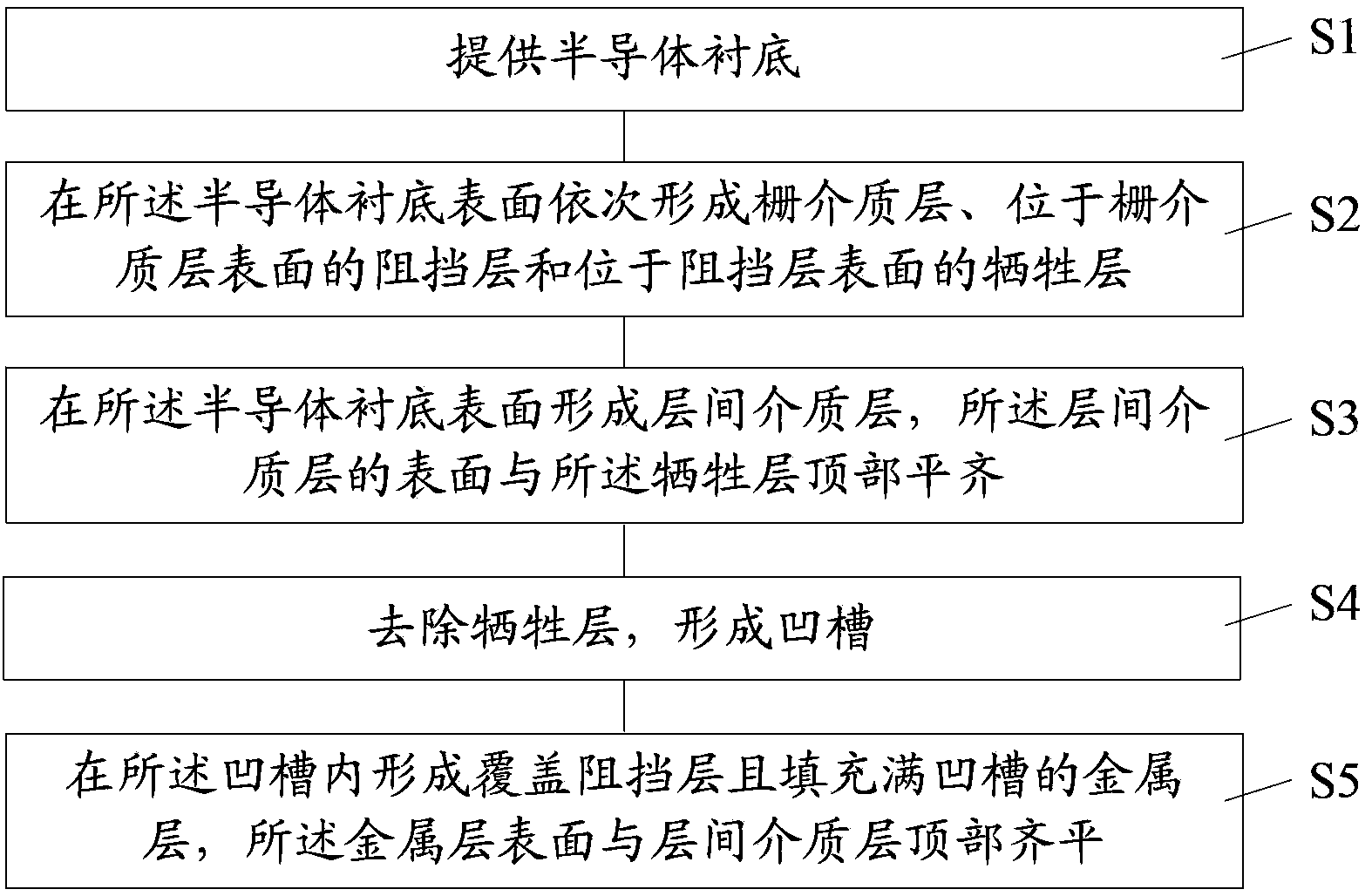
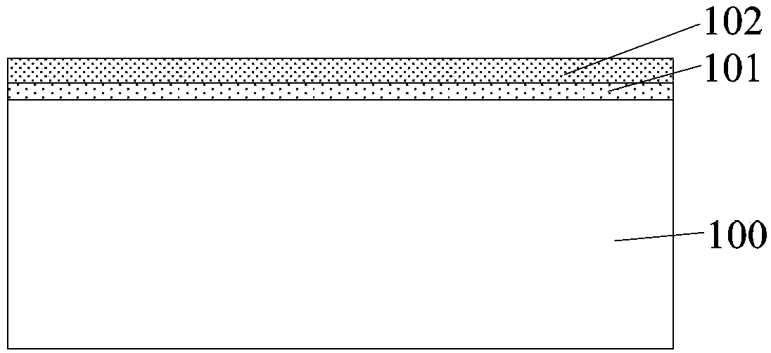
[0034] To this end, the transistor formation process is studied, and it is found that the transistor formation process includes the following steps, please refer to figure 1 : Step S1, providing a semiconductor substrate; Step S2, sequentially forming a gate dielectric layer, a barrier layer on the surface of the gate dielectric layer, and a sacrificial layer on the surface of the barrier layer on the surface of the semiconductor substrate; Step S3, forming a gate dielectric layer on the surface of the semiconductor substrate An interlayer dielectric layer is formed on the bottom surface, and the surface of the interlayer dielectric layer is flush with the top of the sacrificial layer; Step S4, removing the sacrificial layer to form a groove; Step S5, forming a covering barrier layer in the groove and ...


PUM

PropertyMeasurementUnit
Thicknessaaaaaaaaaa

Abstract

Provided is a transistor and a formation method thereof. The formation method of the transistor include: providing a semiconductor substrate; successively forming, on the surface of the semiconductor substrate, a gate dielectric layer, a first barrier layer on the surface of the gate dielectric layer, and a sacrificial layer on the surface of the first barrier layer; forming an interlayer dielectric layer on the surface of the semiconductor substrate, wherein the surface of the interlayer dielectric layer is aligned to the top of the sacrificial layer; removing the sacrificial layer to form a slot; forming a second barrier layer, which covers the first barrier layer, in the slot, wherein the morphology of the second barrier layer and morphology of the first barrier layer on which the sacrificial layer has been removed are in complementation; forming a metal layer fully filling the slot on the surface of the second barrier layer, wherein the surface of the metal layer is aligned to the top of the interlayer dielectric layer. This invention reduces the leakage current of the gate of the transistor and improves the reliability and electrical properties of the transistor.

Description

technical field [0001] The invention relates to the field of semiconductor manufacturing, in particular to a transistor and a method for forming the transistor. Background technique [0002] The main semiconductor device of integrated circuits, especially VLSIs, is metal-oxide-semiconductor field effect transistors (MOS transistors). With the continuous development of integrated circuit manufacturing technology, the technology node of semiconductor devices is continuously reduced, and the geometric size of transistors is continuously reduced following Moore's law. When the size of the transistor is reduced to a certain extent, various secondary effects caused by the physical limit of the transistor appear one after another, and it becomes more and more difficult to scale down the feature size of the transistor. Among them, in the field of transistor and semiconductor manufacturing, the most challenging thing is how to solve the problem of large leakage current of transistor...

Claims


Application Information

Patent Timeline
IPC IPC(8): H01L29/78H01L27/088H01L21/336H01L21/8234
CPCH01L29/42356H01L29/66568H01L29/78
Inventor 李凤莲倪景华
Owner SEMICON MFG INT (SHANGHAI) CORP
Why Eureka
Try Eureka