Semiconductor laser device with stable wavelength and manufacturing method thereof

A laser and semiconductor technology, applied in the direction of semiconductor lasers, lasers, laser parts, etc., can solve the problems of complex technology and high cost, and achieve the effect of reducing wavelength drift, reducing coefficient, structure and manufacturing process.

Inactive Publication Date: 2015-01-21
Shandong Huaguang Optoelectronics Co. Ltd.
View PDF11 Cites 1 Cited by
  • Summary
  • Abstract
  • Description
  • Claims
  • Application Information

AI Technical Summary

Problems solved by technology

[0005] In addition, as disclosed in CN1989666 "Laser Module with Stable Wavelength" and "Laser Wavelength Stabilization Method and Device for Realizing it" disclosed in CN1251692, grating filters and power controllers are used, similar to the grating control in the above 3, and the technology is complicated. High cost, suitable for high-end products

Method used


Image

  • Semiconductor laser device with stable wavelength and manufacturing method thereof
  • Semiconductor laser device with stable wavelength and manufacturing method thereof
  • Semiconductor laser device with stable wavelength and manufacturing method thereof

Examples


Embodiment 1

[0023] This embodiment is the manufacture of TO packaged lasers (including TO56, TO9, etc.), including the following steps:

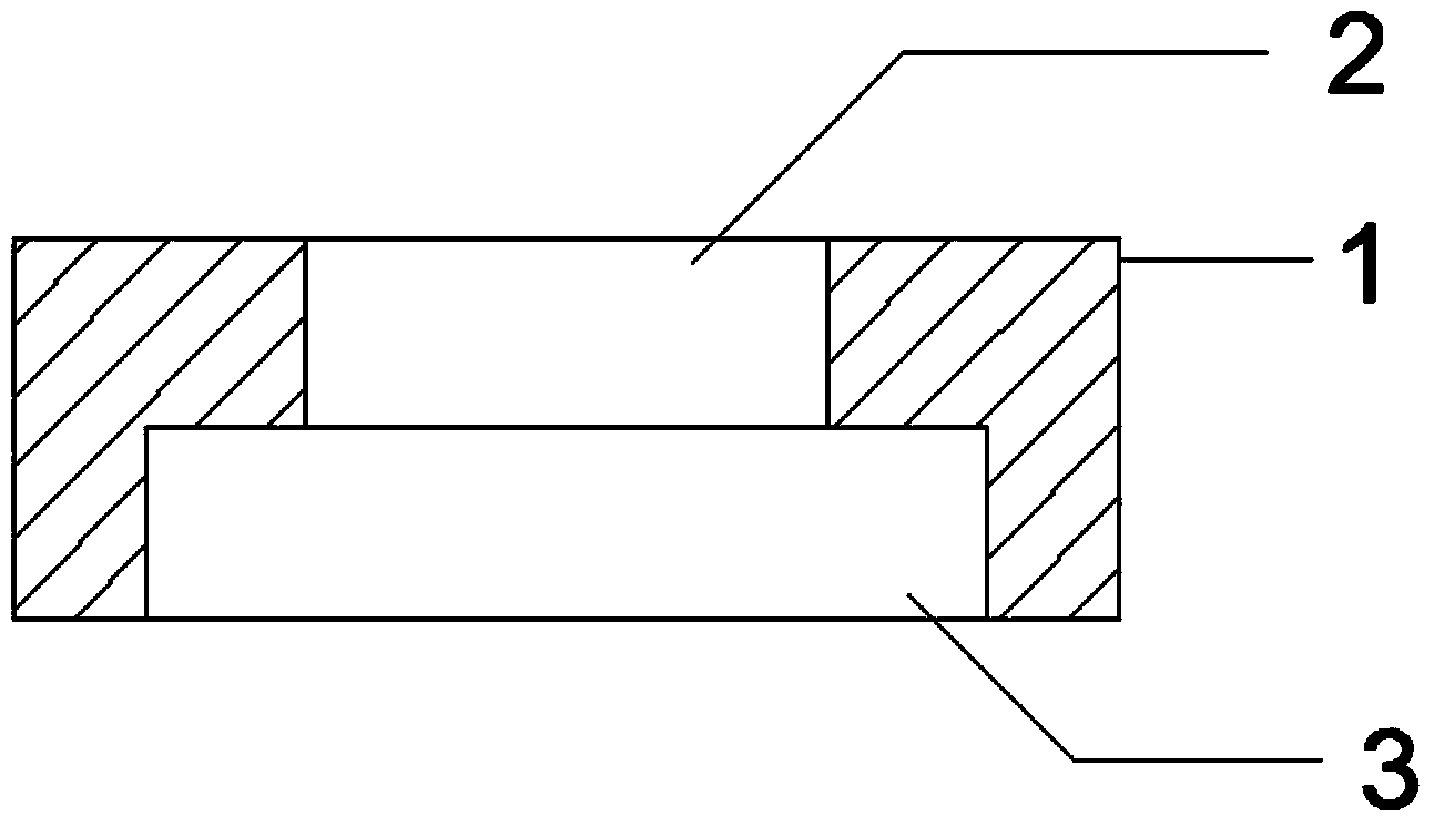
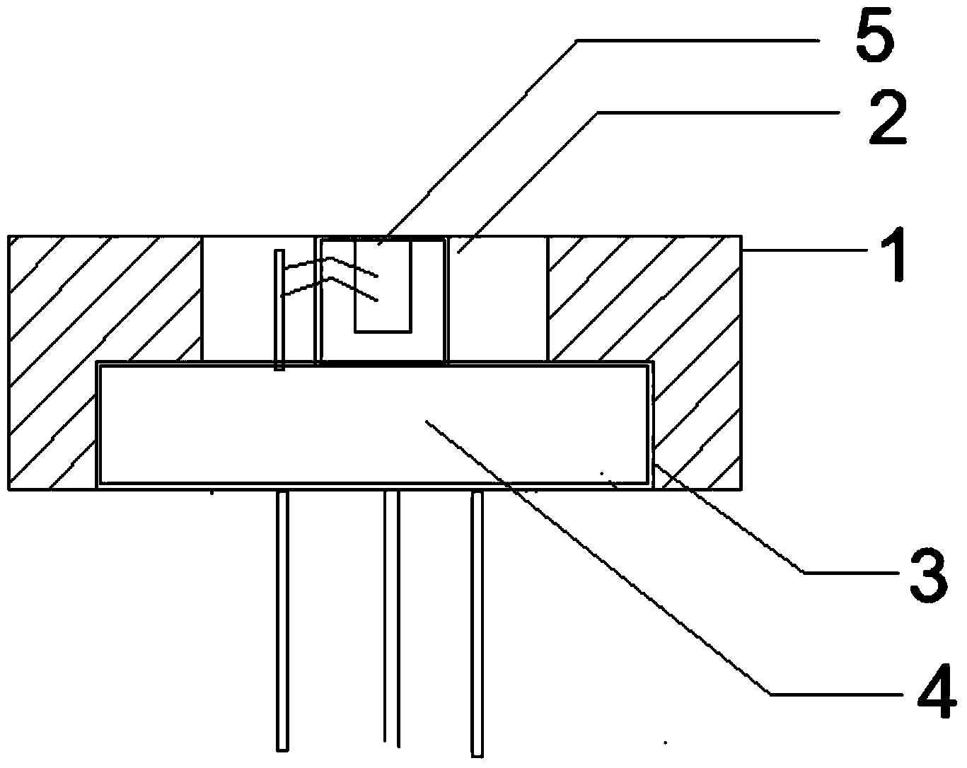
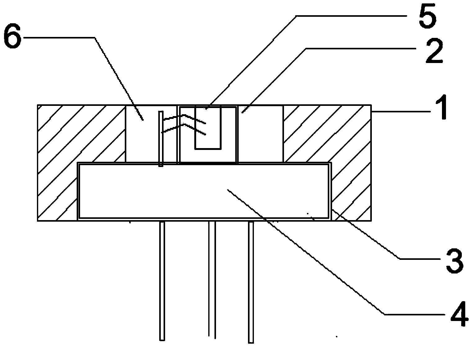
[0024] (1) production figure 1 As shown in the metal base 1 , the base plate is circular or square in shape, with a coaxial large hole 3 and a small hole 2 inside, and the large hole 3 and the small hole 2 form a stepped hole. The diameter of the large hole 3 is slightly smaller than the diameter of the TO base of the TO package laser.

[0025] (2) if figure 2 As shown, assemble the TO package laser 4 into the figure 1 In the large hole 3 of the circular metal substrate 1 shown, the TO socket of the TO packaged laser 4 forms an interference fit with the large hole 3 , and the front cavity surface 5 of the TO packaged laser is flush with the small hole 2 .

[0026] (3) if image 3 As shown, the space of the small hole 2 is filled with a heat-conducting adhesive 6 (curable type such as heat-conducting silica gel), and the height of the heat-conductin...

Embodiment 2

[0032] This embodiment is the manufacture of a C-mount packaged laser, including the following steps:

[0033] (1) production Figure 4 The metal substrate 1 shown has a square or circular shape with a circular or square blind hole 7 inside. The depth of the blind hole 7 is consistent with the height of the C-mount heat sink of the C-mount packaged laser 8 .

[0034] (2) if Figure 5 As shown, the C-mount packaged laser 8 is fixed in the blind hole 7, and the front cavity surface 5 of the C-mount packaged laser 8 is flush with the blind hole 7 (that is, flush with the square metal substrate 1).

[0035] (3) if Image 6 As shown, the space of the blind hole 7 is filled with heat-conducting adhesive, and the height of the heat-conducting adhesive is smaller than the front cavity surface of the C-mount packaged laser 8 .

[0036] (4) Put the laser on the metal substrate 1 in an oven lower than 70°C, and cure it at 60°C-70°C for 20-30 minutes.


PUM


Abstract

The invention relates to a semiconductor laser device with a stable wavelength and a manufacturing method of the semiconductor laser device. The semiconductor laser device comprises a heat conduction substrate and a laser device body, the laser device body is installed in the heat conduction substrate, the front cavity face of the laser device body is flush with the end face of the heat conduction substrate, heat conduction glue is poured into the portion between the laser device body and the heat conduction substrate, and the height of the heat conduction glue is smaller than that of the front cavity face of the laser device body. The manufacturing method includes the steps that (1), the heat conduction substrate is manufactured; (2), the laser device body is installed in an installing hole of the laser device body of the heat conduction substrate, and the front cavity face of the laser device body is flush with the installing hole of the laser device body; (3), the heat conduction glue is poured into the space between the laser device body and installing hole of the laser device body, and the height of the heat conduction glue is smaller than that of the front cavity face of the laser device body; (4), the heat conduction glue is solidified. The semiconductor laser device is simple in structure, the manufacturing process is simple, heat of a chip of the laser device is dissipated through the heat conduction glue in time, particularly, heat of a rear cavity face is dissipated in time, the factor, of the wavelength change along with temperature, of the laser device can be reduced, wavelength shift of the laser device can be reduced by over 60%, and the wavelength stability is improved.

Description

technical field [0001] The invention relates to a semiconductor laser with stable wavelength and a manufacturing method thereof, belonging to the technical field of semiconductor laser packaging. Background technique [0002] Semiconductor lasers have the advantages of high efficiency, long life, high beam quality, good stability, and compact structure. They are widely used in optical fiber communication, laser pumping, medical equipment, optical image processing, laser printers and other fields. With the increasing development and maturity of semiconductor technology, laser diodes have been greatly improved in terms of power, conversion efficiency, wavelength extension and operating life. Since the semiconductor laser has the characteristics of high quantum efficiency, high reliability, long service life, good correspondence between the emission wavelength and the absorption peak of the laser medium, and good quality of the laser output beam, it is beneficial to combine wit...

Claims


Application Information

Patent Timeline
IPC IPC(8): H01S5/024H01S5/0687
Inventor 苏建李沛旭于果蕾邵慧慧刘成成徐现刚
Owner Shandong Huaguang Optoelectronics Co. Ltd.
Why Eureka
Try Eureka