Silicon substrate integrated coherent light transmitter chip and transmitter

A transmitter and coherent light technology, applied in the direction of electromagnetic transmitters, etc., can solve the problem that single-drive silicon-based modulators are difficult to modulate signals with a large extinction ratio, cannot achieve equal polarization signal power, and output amplitude of high-frequency RF signal amplifiers Limited problems, to overcome the influence of work stability and connection stability between devices, simple structure, and compatible processing technology

Active Publication Date: 2015-01-21
PEKING UNIV
View PDF5 Cites 12 Cited by
  • Summary
  • Abstract
  • Description
  • Claims
  • Application Information

AI Technical Summary

Problems solved by technology

[0005] Among them, although the single-drive silicon-based modulator has the advantage of using fewer RF drive signal channels, since the single-channel RF signal voltage needs to be loaded on two modulators for driving, the output amplitude of the single-channel RF signal is required to be high. At present, the half-wave voltage of silicon-based modulators is generally large, and the output amplitude of high-frequency RF signal amplifiers is limited. It is difficult to achieve a large extinction ratio and obtain high-quality modulation signals with single-drive silicon-based In order to ac

Method used


Image

  • Silicon substrate integrated coherent light transmitter chip and transmitter
  • Silicon substrate integrated coherent light transmitter chip and transmitter
  • Silicon substrate integrated coherent light transmitter chip and transmitter

Examples


Embodiment Construction

[0038] The present invention will be described in further detail below in conjunction with the accompanying drawings and embodiments. The following examples are used to illustrate the present invention, but should not be used to limit the scope of the present invention.

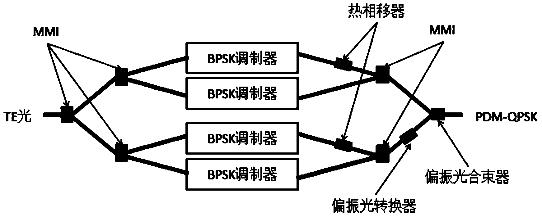
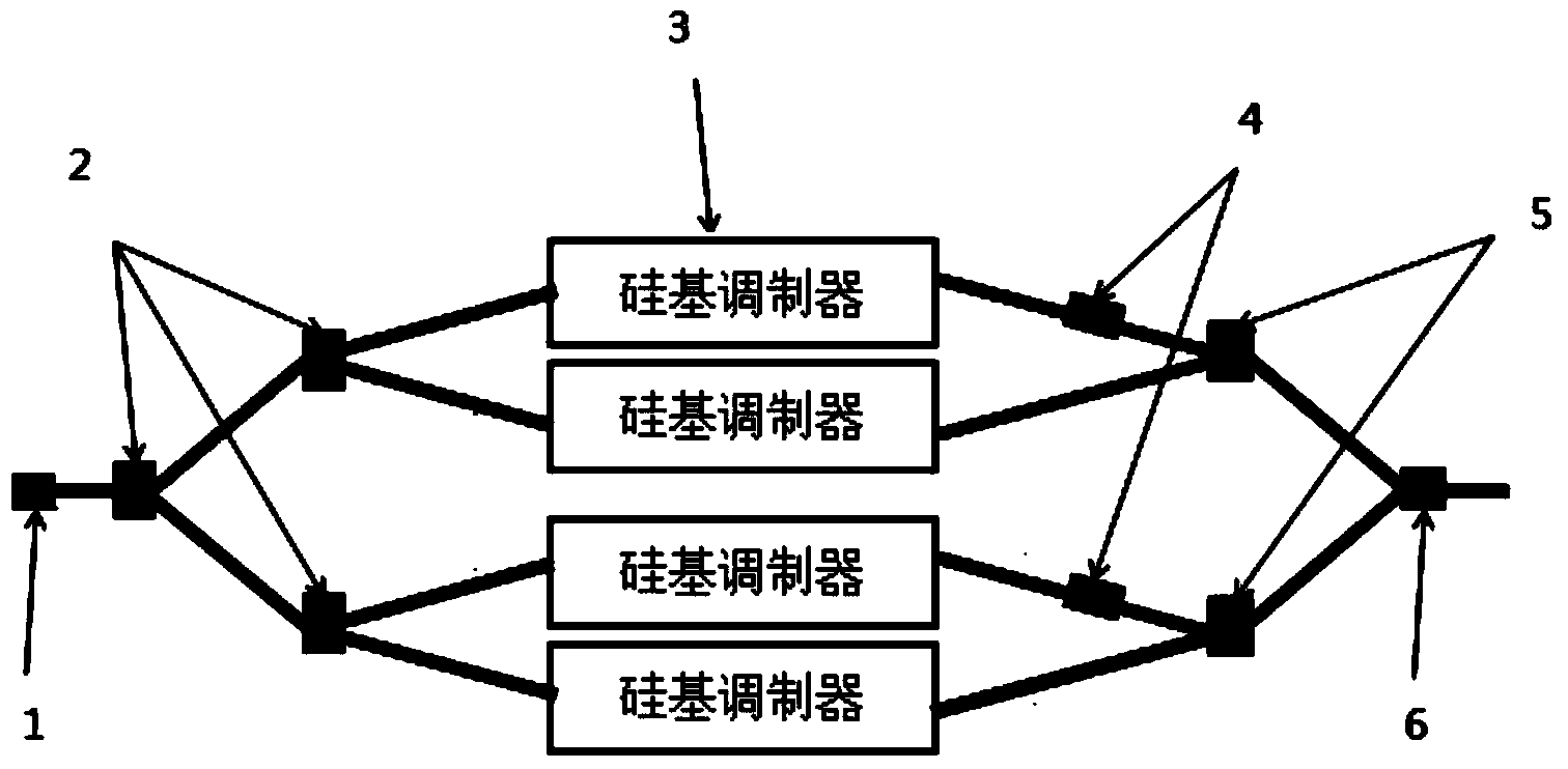
[0039] The invention discloses a silicon-based integrated coherent optical transmitter chip, such as figure 2 As shown, it includes an optical coupler 1, an optical beam splitter 2, an optical beam combiner 5, a silicon-based modulator 3, a fixed phase shifter 4, and a coupling polarization beam combiner 6;

[0040] The TE polarized light is coupled into the planar optical waveguide by the optical coupler 1, and is divided into four beams of light with equal power by the optical beam splitter 2, and then respectively enters a silicon-based modulator 3 for processing and then outputs the first A modulated signal light, a second modulated signal light, a third modulated signal light and a fourth modulated sig...


PUM


Abstract

The invention discloses a silicon substrate integrated coherent light transmitter chip and a transmitter. The silicon substrate integrated coherent light transmitter chip comprises an optical coupler, a light beam splitter, a light beam combining device, a silicon substrate modulator, a fixed phase drift device and a coupling polarization beam combining device. The optical coupler is used for achieving coupling of input end light. The light beam splitter and the light beam combining device are used for achieving the beam splitting and beam combining functions of optical signals. The silicon substrate modulator is a core modulator part, and is used for achieving the function of loading electrical signals to the optical signals, and generation of modulation signal light is finished. The fixed phase drift device is used for achieving fixed rotating of the phase position of the optical signals. The coupling polarization beam combining device is used for combining two paths of signal light with the transverse electric (TE) polarization state into one path of transverse electric and magnetic field (TEM) signal light. The silicon substrate integrated coherent light transmitter chip and the transmitter are suitable for an optical communication system with multi-phase-position modulating and polarization multiplexing, and have the advantages that cost is low, the CMOS technology is compatible, achieving is easy, integrity is high, and packaging is easy.

Description

technical field [0001] The invention relates to the technical field of coherent optical transmitters, and more specifically relates to a silicon-based integrated coherent optical transmitter chip and a transmitter. Background technique [0002] Optical communication is developing towards a high-speed optical transmission system with higher spectral efficiency, lower energy consumption, longer distance, and larger capacity. At present, driven by the continuous development of high-bandwidth new services, the application requirements based on 100Gb / s high-speed transmission are becoming more and more obvious. Typical examples include Huawei's 100Gb / s deployment in the Royal Dutch KPN Telecom Group, Aaron's 100Gb / s upgrade in France's Completel, and Hong Kong's New World Telecom's 100G deployment. After the first round of test and verification in China, the construction of commercial networks has begun. Among them, China Mobile has taken the lead in conducting large-scale bidd...

Claims


Application Information

Patent Timeline
IPC IPC(8): H04B10/50
Inventor 周治平王兴军张俊龙李田甜余丽苏昭棠
Owner PEKING UNIV
Why Eureka
Try Eureka