Storage device and data reading-writing method thereof

A storage device, data reading and writing technology, applied in the field of micro-nano electronics, can solve problems such as inability to rewrite, and achieve the effect of avoiding data loss, reducing damaged sectors, and realizing the function of bad block shielding

Active Publication Date: 2015-01-28
SHANGHAI INST OF MICROSYSTEM & INFORMATION TECH CHINESE ACAD OF SCI
View PDF5 Cites 10 Cited by
  • Summary
  • Abstract
  • Description
  • Claims
  • Application Information

AI Technical Summary

Problems solved by technology

[0005] In view of the above-mentioned shortcomings of the prior art, the purpose of the present invention is to provide a storage device and its data reading and writing method, which is used to solve the problem that the SD card in the prior art must perform a block erase operation before writing data, and cannot realize " rewrite" problem

Method used


Image

  • Storage device and data reading-writing method thereof
  • Storage device and data reading-writing method thereof
  • Storage device and data reading-writing method thereof

Examples


Embodiment Construction

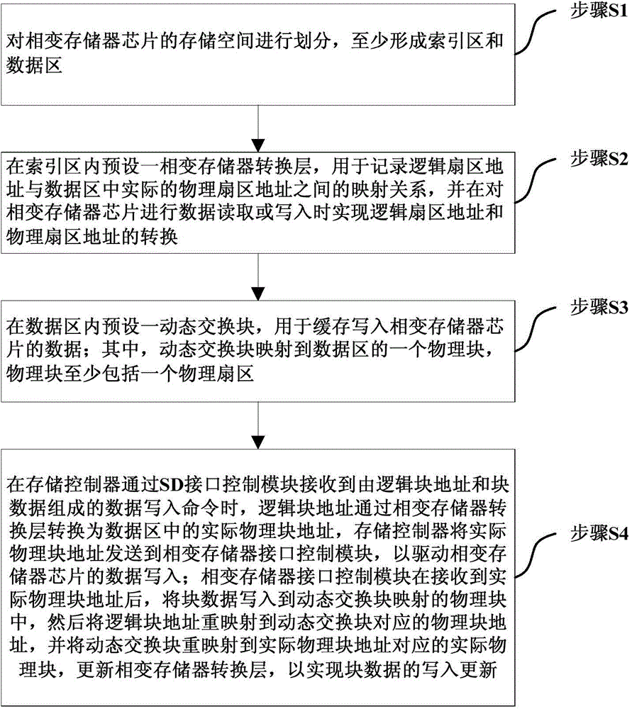
[0046] Embodiments of the present invention are described below through specific examples, and those skilled in the art can easily understand other advantages and effects of the present invention from the content disclosed in this specification. The present invention can also be implemented or applied through other different specific implementation modes, and various modifications or changes can be made to the details in this specification based on different viewpoints and applications without departing from the spirit of the present invention.

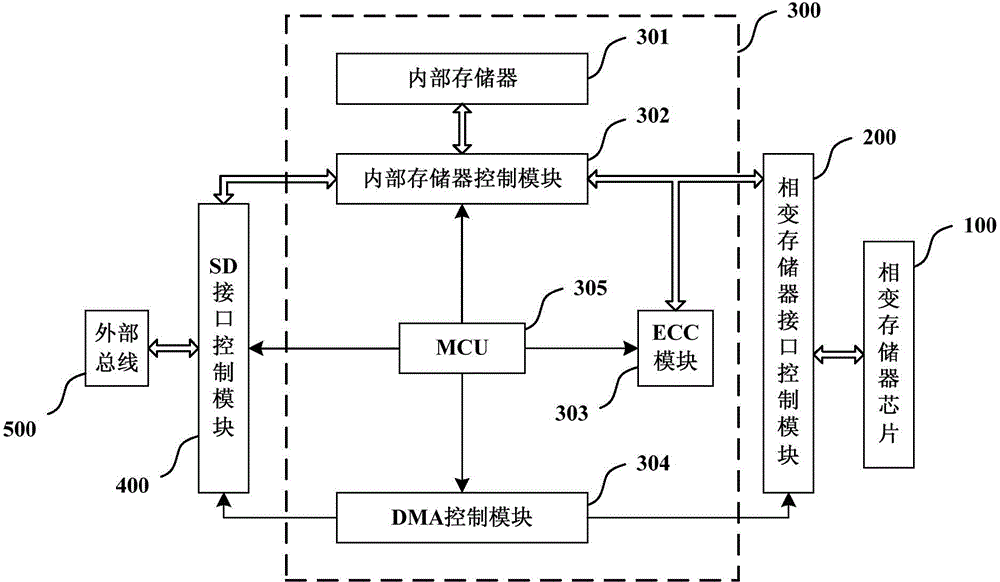
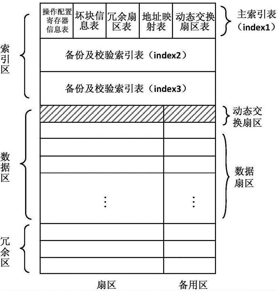
[0047] seefigure 1 , the first embodiment of the present invention relates to a storage device. It should be noted that the diagrams provided in this embodiment are only schematically illustrating the basic idea of ​​the present invention, and only the components related to the present invention are shown in the diagrams rather than the number, shape and shape of the components in actual implementation. Dimensional drawing, the type, ...


PUM


Abstract

The invention provides a storage device and a data reading-writing method thereof. The storage device at least comprises a phase change memory chip, a phase change memory interface control module, an SD (secure digital) interface control module and a storage controller. The phase change memory interface control module is coupled to the phase change memory chip. The SD interface control module is coupled to an external device. The storage controller is coupled to the phase change memory interface control module and the SD interface control module. The storage controller is used for responding to a data reading or writing command from the SD interface control module and controlling reading or writing of the phase change memory chip through the phase change memory interface control module. The storage device is an SD card based on a phase change memory; the phase change memory chip is used as a storage medium allowing random reading and writing. Additionally, compared with flashes, the storage device and the data reading-writing method thereof have the advantages that operations such as bad block management and ECC (error checking and correcting) are simpler, a function of shielding bad blocks is achieved, and fatigue is resisted.

Description

technical field [0001] The invention relates to the technical field of micro-nano electronics, in particular to a storage device and a data reading and writing method thereof. Background technique [0002] Phase Change Random Access Memory (PCRAM) is a new type of non-volatile random access memory. Its basic principle is to use chalcogenide compounds as storage media, and make phase change materials in polycrystalline (low resistance ) and the amorphous (high resistance) state, and use the difference between the two states to represent binary data. PCRAM is fully compatible with CMOS standard technology in terms of technology, and has the characteristics of fast operation speed, good fatigue resistance and miniaturization, and has very broad commercial prospects in terms of low voltage, low power consumption, high speed, high density and embedded storage. . PCRAM is considered to be the next-generation non-volatile memory that is most likely to replace flash memory (FLASH)...

Claims


Application Information

Patent Timeline
Patent Type & Authority Applications(China)
IPC IPC(8): G06F13/28G06F12/06
Inventor 王月青陈小刚蔡道林宋志棠李喜陈一峰
Owner SHANGHAI INST OF MICROSYSTEM & INFORMATION TECH CHINESE ACAD OF SCI
Why Eureka
Try Eureka