Electrostatic discharge protection method of chip with multiple power systems and multiple package types

A technology of power supply system and chip, which is applied in the direction of circuits, electrical components, electric solid devices, etc., can solve the problems of high substrate potential, damage of internal devices, increase of chip area, etc., and achieve the effect of small chip area

Inactive Publication Date: 2015-02-11
BEIJING CEC HUADA ELECTRONIC DESIGN CO LTD
View PDF3 Cites 7 Cited by
  • Summary
  • Abstract
  • Description
  • Claims
  • Application Information

AI Technical Summary

Problems solved by technology

However, this method will increase the chip area
More importantly, since the ESD ground path is led to the inside of the chip, the substrate potential inside the chip may be too high, which may cause damage to internal devices during ESD discharge

Method used


Image

  • Electrostatic discharge protection method of chip with multiple power systems and multiple package types
  • Electrostatic discharge protection method of chip with multiple power systems and multiple package types

Examples


Embodiment Construction

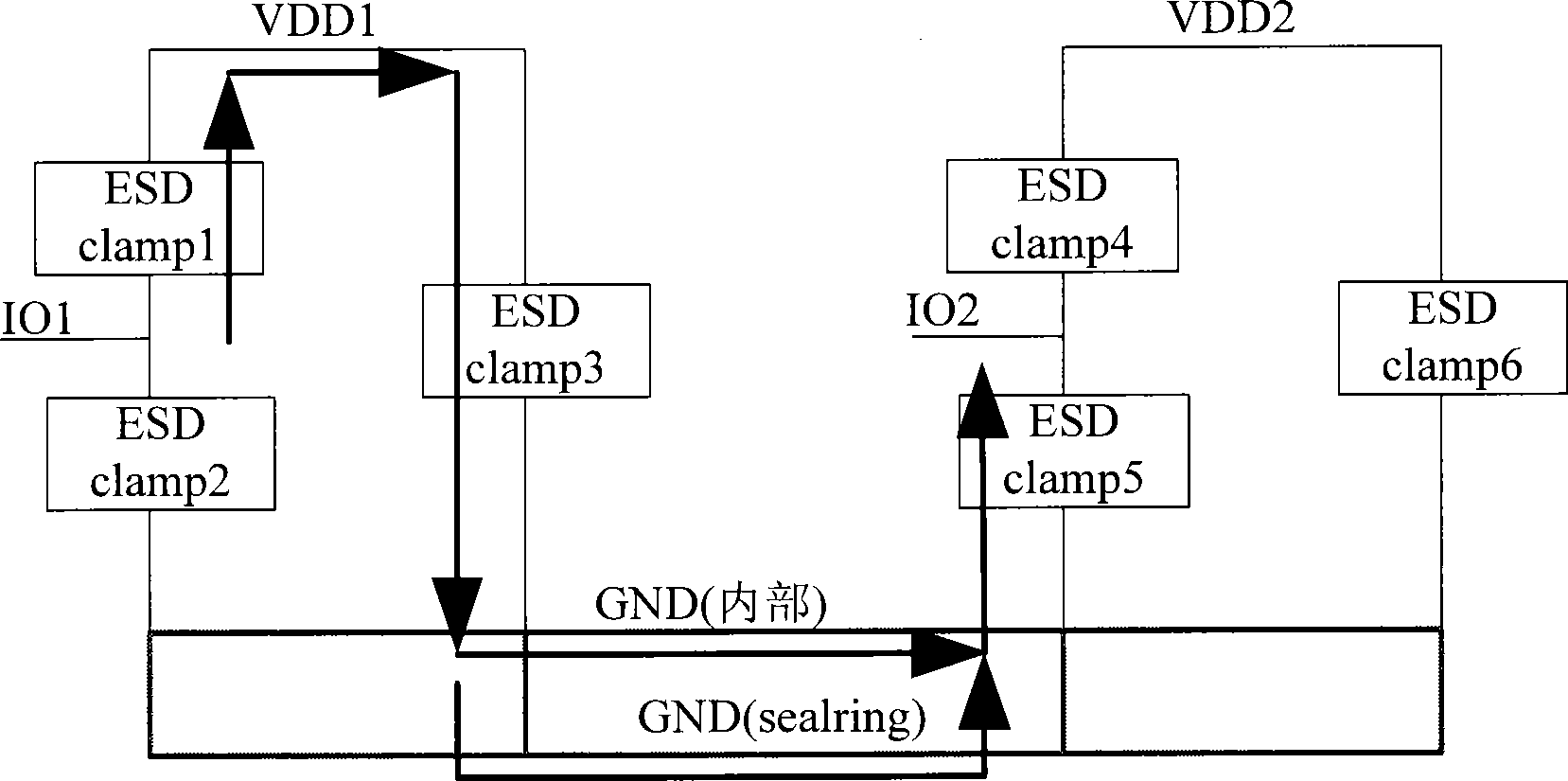
[0019] Such as figure 1 As shown, the ESD current of IO1 pin flows to VDD1 through ESD clamp1, flows to GND inside the chip through ESD clamp3, and flows to sealring GND at the same time, GND inside the chip and sealring GND form a parallel path, and reaches the GND node of IO2. Foot discharge.

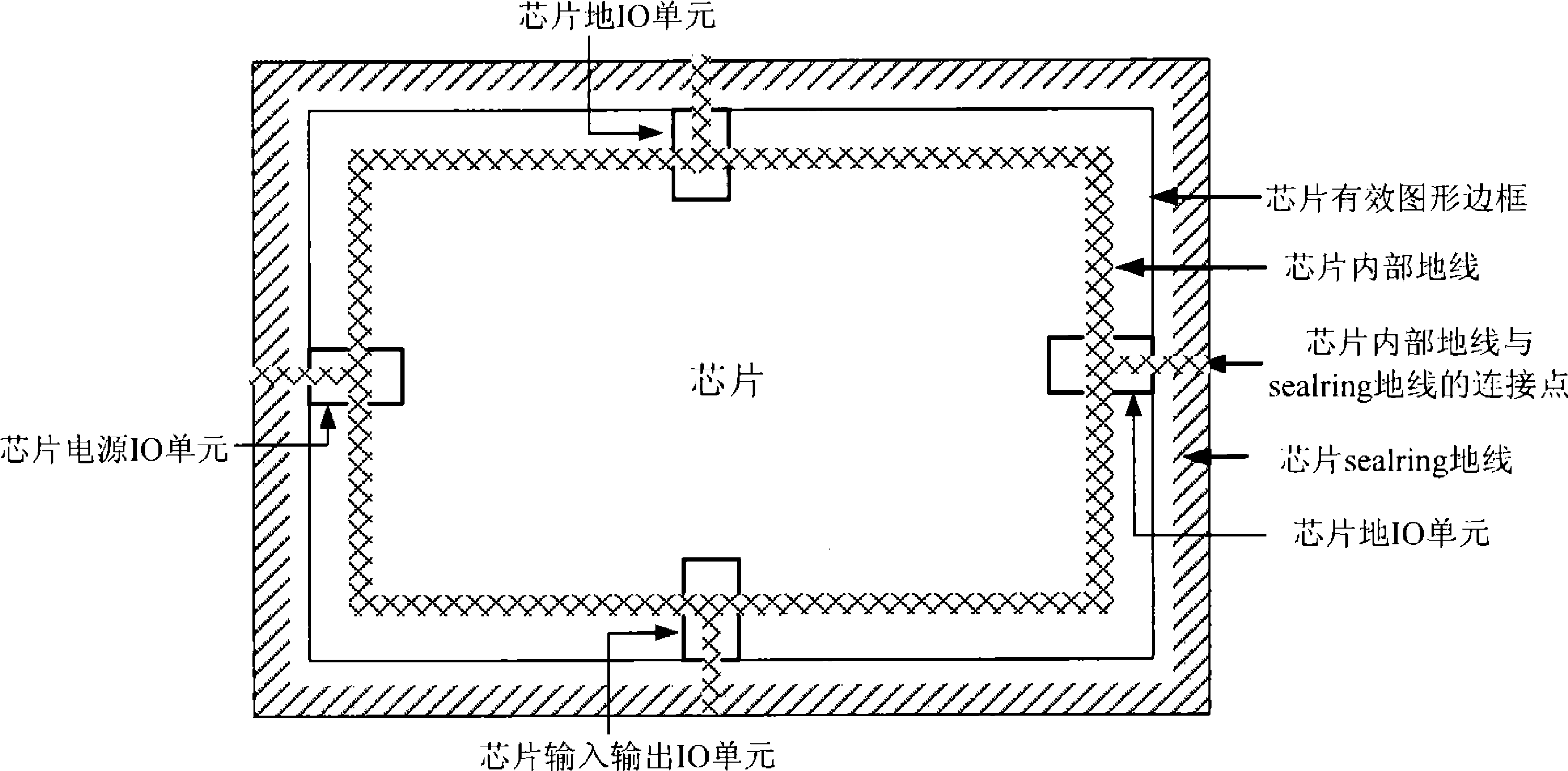
[0020] Such as figure 2 As shown, taking a chip with an area of ​​4mm*4mm as an example, the internal ground wire of the chip is metal2, the width is 40um, and it is closed to form a ring in the chip; the ground wire of the seal ring outside the chip is metal1~metal4, and the width is 10um. As shown in the figure, the black line is the effective graphic frame of the chip; the slanted line is the sealring of the outer ring of the chip; the grid line is the annular ground wire inside the chip and the ground wire connected to the sealring. The connection between each IO and the sealring can be connected according to the number of metal layers and the metal width actually allowed by th...


PUM


Abstract

The invention discloses an electrostatic discharge protection method of a chip with multiple power systems and multiple package types. According to the method, in addition to using a common ground wire path in the chip, a ground potential in a seal ring is utilized, and a ground wire of each power system is connected, so that the electrostatic discharge current is released through two parallel paths, and thus the condition of damage caused by excessive potential of a circuit in the chip due to overlarge parasitic resistance on a discharge path is avoided. According to the method, the ESD (Electronic Static Discharge) performance of the chip is enhanced without increasing the area of the chip.

Description

technical field [0001] The invention proposes a chip electrostatic discharge protection method with multiple power supply systems and multiple packaging forms. The invention is applicable to the field of chip design with multiple power supply systems and multiple packaging forms, and is especially suitable for chip design with IOs sharing the same ground potential. Background technique [0002] As the integrated circuit manufacturing process level enters the deep submicron era, the MOS (metal-oxide-semiconductor) transistors in the integrated circuit all adopt the lightly doped structure LDD (Lightly Doped Drain); the silicide process covers the diffusion area of ​​the MOS transistor ; The polycrystalline compound process can reduce the series resistance of the gate polycrystal; the thickness of the gate oxide layer of the MOS transistor is getting thinner and the channel length is getting smaller and smaller. These improvements have improved the integration level of the ch...

Claims


Application Information

Patent Timeline
Patent Type & Authority Applications(China)
IPC IPC(8): H01L27/02H01L23/60
Inventor 张颖李志国潘亮
Owner BEIJING CEC HUADA ELECTRONIC DESIGN CO LTD
Why Eureka
Try Eureka