Thin-film transistor array substrate

A technology of thin film transistors and array substrates, which is applied in the field of display panels and can solve the problems of limited pixel aperture ratio of liquid crystal display panels

Active Publication Date: 2015-02-11
HANNSTAR DISPLAY CORPORATION
View PDF4 Cites 9 Cited by
  • Summary
  • Abstract
  • Description
  • Claims
  • Application Information

AI Technical Summary

Problems solved by technology

[0005] However, the pixel aperture ratio of liquid crystal display panels formed by such TFT array substrates is still limited.

Method used


Image

  • Thin-film transistor array substrate
  • Thin-film transistor array substrate
  • Thin-film transistor array substrate

Examples


Embodiment Construction

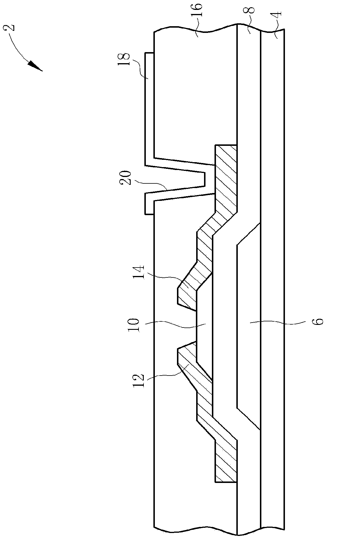
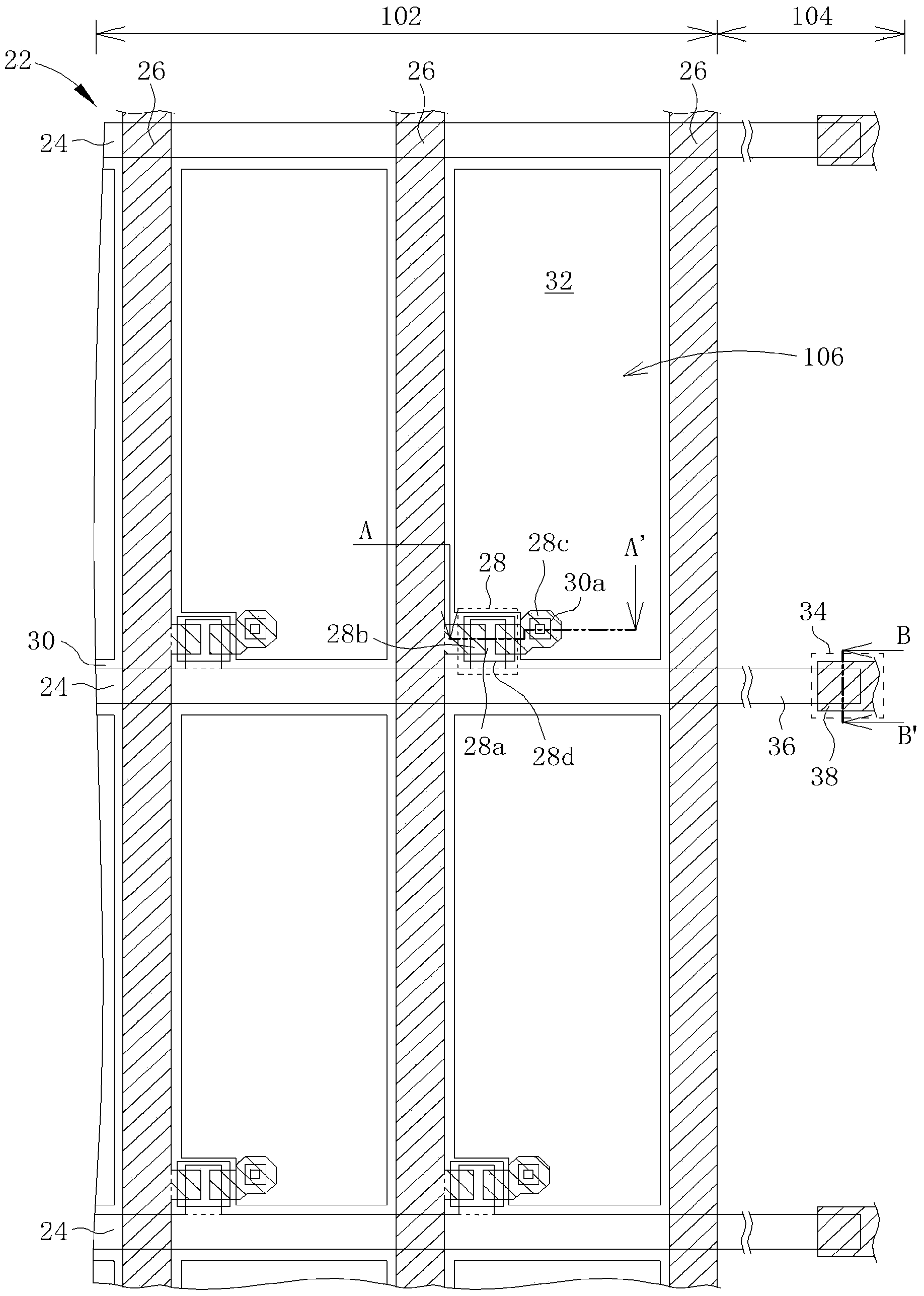
[0023] figure 2 A schematic bottom view showing a thin film transistor array substrate according to an embodiment of the present invention. The TFT array substrate 22 includes a display area 102 and a fan-out area 104 . In the display area 102 , there are a plurality of scan lines 24 , a plurality of data lines 26 , a plurality of thin film transistors 28 , a common electrode 30 and a plurality of pixel electrodes 32 . The data lines 26 and the scan lines 24 intersect, so that any two adjacent data lines 26 and any two adjacent scan lines 24 surround a pixel region 106 , and the pixel regions 106 are arranged in an array. Each thin film transistor 28 is respectively disposed corresponding to each pixel region 106, and each thin film transistor 28 includes a gate 28a, a source 28b, and a drain 28c, and also includes a gate insulating layer (not shown) and a semiconductor layer 28d. Moreover, the gate electrode 28 a is electrically connected to the corresponding scan line 24 ...


PUM


Abstract

The present invention discloses a thin film transistor array substrate comprising a plurality of thin film transistors, with each one thereof including a gate electrode, a gate insulation layer, an amorphous-oxide semiconductor layer and a pair of a source electrode and a drain electrode. The amorphous-oxide semiconductor layer comprises an amorphous-oxide semiconductor material having a-IGZO. The thin film transistor array substrate further comprises a first insulation layer and a second insulation layer disposed on the thin film transistors. Since the a-IGZO semiconductor layer and the thick insulation layer covered thereon are used in the present invention, a common electrode can overlap the scan lines or data lines to increase the aperture ratio of the pixel structure. Furthermore, the thick insulation layer can be fabricated through a coating process, so as to keep the a-IGZO semiconductor layer from damages during the fabrication processes.

Description

technical field [0001] The present invention relates to a display panel, in particular to a thin film transistor (thin film transistor, TFT) array (array) substrate. Background technique [0002] Thin-film transistors have been widely used in active array flat display panels, such as active liquid crystal display panels or active organic electroluminescent display panels, as active components to drive each pixel of the display panel structure. The structure of the thin film transistor in the prior art is mainly based on a bottom gate structure, which includes a gate disposed on a substrate, a gate insulating layer covering the gate, a semiconductor layer (semiconductor layer) as a transistor channel, and The source and the drain are respectively disposed on two sides of the semiconductor layer. The main structures of thin film transistors include, for example, inverted co-planar (inverted co-planar), back channel etching (BCE) and channel protection (CHP) and so on. IGZO ...

Claims


Application Information

Patent Timeline
Patent Type & Authority Applications(China)
IPC IPC(8): H01L27/12G02F1/1362G02F1/1368
CPCH01L29/78693H01L27/1225
Inventor 游家华胡宪堂任珂锐赖瑞麒
Owner HANNSTAR DISPLAY CORPORATION
Why Eureka
Try Eureka