Check patentability & draft patents in minutes with Patsnap Eureka AI!

LDMOS (Laterally Diffused Metal Oxide Semiconductor) device with shielding ring and preparation method thereof

A shielding ring and device technology, applied in semiconductor/solid-state device manufacturing, semiconductor devices, electrical components, etc., can solve problems such as failure to optimize the breakdown voltage of radio frequency devices, and achieve the effect of changing the breakdown voltage and optimizing performance

Inactive Publication Date: 2015-02-11
SHANGHAI LIANXING ELECTRONICS
View PDF4 Cites 2 Cited by
  • Summary
  • Abstract
  • Description
  • Claims
  • Application Information

AI Technical Summary

Problems solved by technology

[0014] The purpose of the embodiments of the present invention is to provide an LDMOS device with a shielding ring and its preparation method, so as to solve the problem in the prior art that the breakdown voltage of radio frequency devices cannot be optimized

Method used


Image

  • LDMOS (Laterally Diffused Metal Oxide Semiconductor) device with shielding ring and preparation method thereof
  • LDMOS (Laterally Diffused Metal Oxide Semiconductor) device with shielding ring and preparation method thereof
  • LDMOS (Laterally Diffused Metal Oxide Semiconductor) device with shielding ring and preparation method thereof

Examples


Embodiment 1

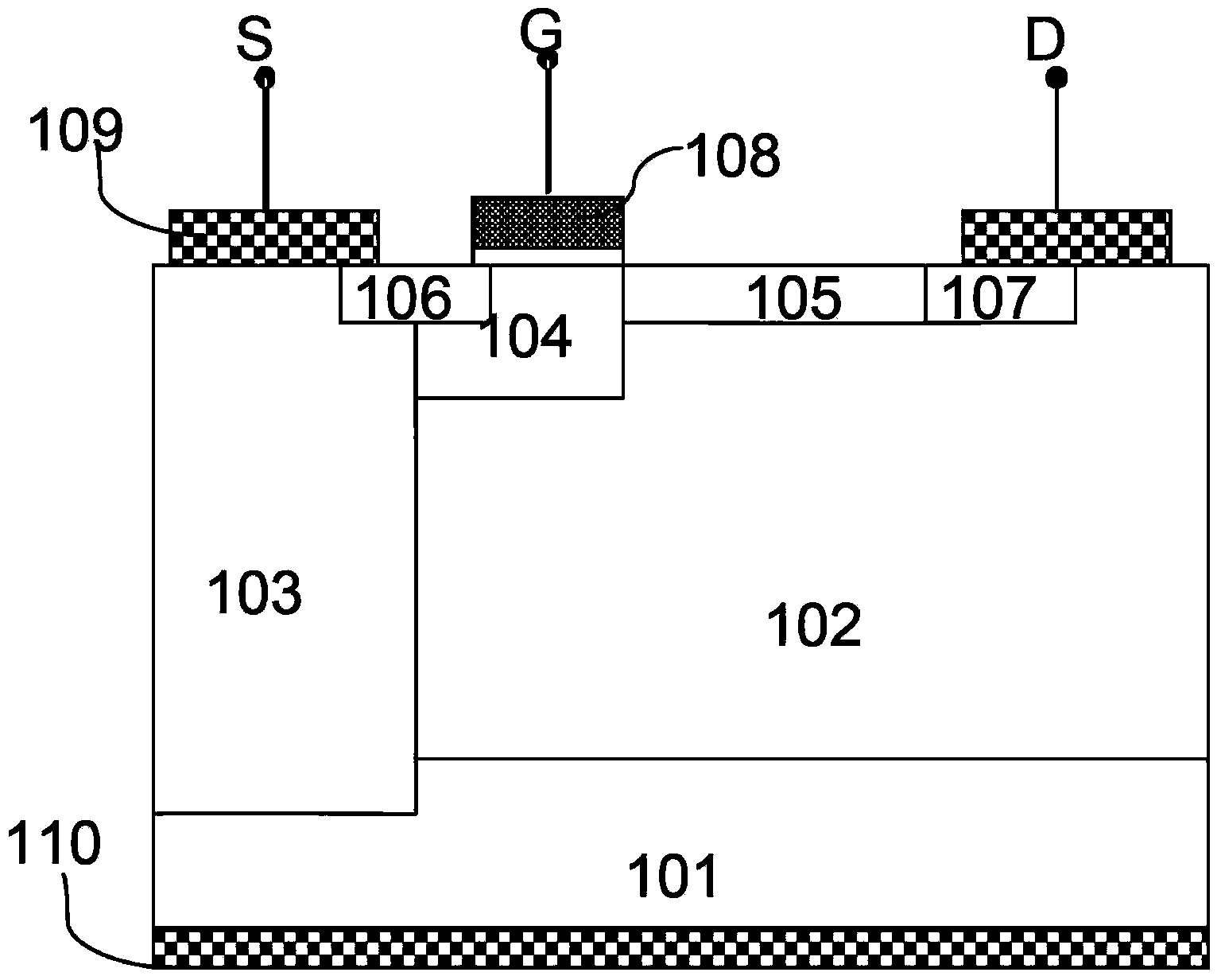
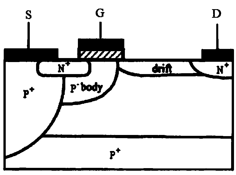
[0041] Such as figure 2 Shown is the schematic diagram of the structure of the LDMOS device obtained through the simulation of the ISE TCAD process provided by the embodiment of the present invention. The structure diagram of the LDMOS device is as follows image 3 As shown, for ease of description, only the parts related to the embodiment of the present invention are shown, including:

[0042] Resistivity 0.05~0.15Ω / cm 3 P+ silicon substrate.

[0043] In an embodiment of the present invention, a radio frequency LDMOS (Lateral Double-diffused MOS, referred to as: lateral double-diffused field effect transistor) device is fabricated on a P+ silicon substrate, and the radio frequency LDMOS device first includes: a resistivity of 0.05 to 0.15Ω / cm 3 P+ silicon substrate.

[0044] Epitaxially formed on the P+ silicon substrate with a thickness of 9 μm and a doping concentration of 6*10 14 cm -3 ~8*10 14 cm -3 The P-type epitaxial region.

[0045] In the embodiment of the...

Embodiment 2

[0090] A flowchart of a method for preparing a light-shielding device provided in an embodiment of the present invention, the method includes the following steps:

[0091] The resistivity of the preparation is 0.05~0.15Ω / cm 3 P+ silicon substrate;

[0092] Formed by epitaxy on the P+ silicon substrate with a thickness of 9 μm and a doping concentration of 6*10 14 cm -3 ~8*10 14 cm -3 The P-type epitaxial region;

[0093] The B impurity implantation dose of the P well formed in the P-type epitaxial region is 2*10 13 cm -2 ~4*10 13 cm -2, The channel area with energy of 40-60Kev and high-temperature propulsion time of 40-60min at 1000-1100°C;

[0094] forming a source region with a field oxygen thickness of 1.8-2.2 μm through the N+ doped region formed in the P well;

[0095] The As impurity implantation dose formed in the N-doped region in the P-type epitaxial region is 1.1*10 12 cm -2 ~1.5*10 12 cm -2 . A drift region with an energy of 140-160Kev, a high-temperat...


PUM

PropertyMeasurementUnit
Lengthaaaaaaaaaa
Lengthaaaaaaaaaa

Abstract

The invention relates to an LDMOS (Laterally Diffused Metal Oxide Semiconductor) device with a shielding ring and a preparation method of the LDMOS device. The invention is applicable to the field of integrated circuit manufacturing and provides the LDMOS device with the shielding ring and the manufacturing method of the LDMOS device. The device comprises a P+ silicon substrate, a P-type epitaxial region, a channel region, a source region, a drift region, a drain region, gate polysilicon and the shielding ring, wherein the P-type epitaxial region is epitaxially forms on the P+ silicon substrate. According to the embodiment of the invention, the breakdown voltage of a radio-frequency LDMOS device is changed by adding the shielding ring to the LDMOS device, so that the performance of the radio-frequency LDMOS device is optimized.

Description

technical field [0001] The invention belongs to the field of integrated circuits, in particular to an LDMOS device with a shielding ring and a preparation method thereof. Background technique [0002] Lateral Double-diffused MOS (LDMOS) is a radio frequency power device with great market demand and broad development prospects. In the field of radio frequency wireless communication, base stations and long-distance transmitters almost all use silicon-based LDMOS high-power transistors; in addition, LDMOS is also widely used in radio frequency amplifiers, such as HF, VHF and UHF communication systems, pulse radar, industrial, scientific and medical applications , Avionics and WiMAXTM communication systems and other fields. Because LDMOS has the advantages of high gain, high linearity, high withstand voltage, high output power, and easy compatibility with CMOS technology, silicon-based LDMOS transistors have become a new hot spot in radio frequency semiconductor power devices. ...

Claims


Application Information

Patent Timeline
IPC IPC(8): H01L29/78H01L29/06H01L21/336
CPCH01L29/7816H01L29/0607H01L29/66681
Inventor 杜寰
Owner SHANGHAI LIANXING ELECTRONICS
Features
  • R&D
  • Intellectual Property
  • Life Sciences
  • Materials
  • Tech Scout
  • Unparalleled Data Quality
  • Higher Quality Content
  • 60% Fewer Hallucinations
Learn More