PCB (Printed Circuit Board) and manufacturing method thereof

A technology for printed circuit boards and manufacturing methods, applied in the fields of printed circuit manufacturing, printed circuits, printed circuit components, etc., can solve the problems of incomplete PP powder treatment and PP powder residue, so as to improve production quality and overcome PP powder residue Effect

Inactive Publication Date: 2015-02-11
PEKING UNIV FOUNDER GRP CO LTD +3
View PDF8 Cites 11 Cited by
  • Summary
  • Abstract
  • Description
  • Claims
  • Application Information

AI Technical Summary

Problems solved by technology

[0006] However, the method of wiping the board surface with a wet wax cloth may not completely treat the PP powder, and there are still PP powder residues in some graphics

Method used


Image

  • PCB (Printed Circuit Board) and manufacturing method thereof
  • PCB (Printed Circuit Board) and manufacturing method thereof
  • PCB (Printed Circuit Board) and manufacturing method thereof

Examples


Embodiment Construction

[0027] The present invention will be described in detail below with reference to the accompanying drawings and in combination with embodiments.

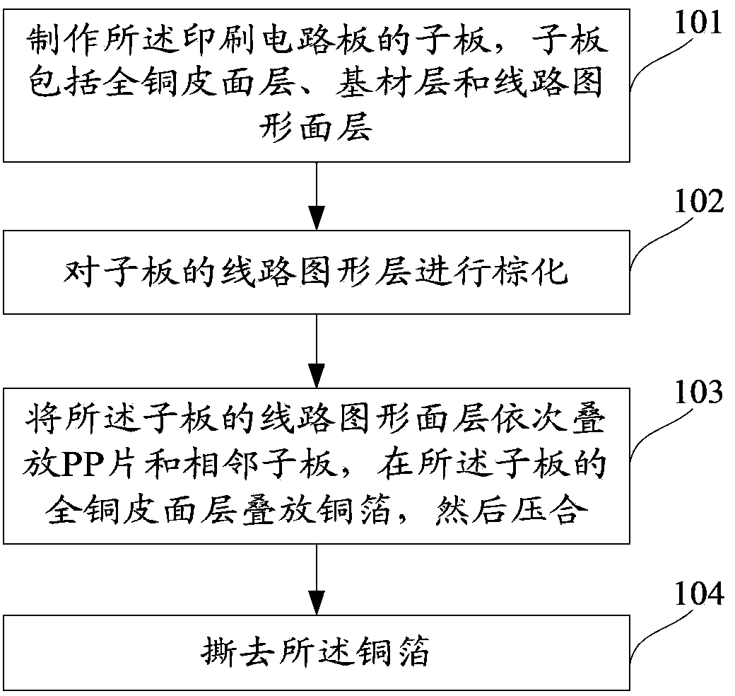
[0028] One embodiment of the present invention provides a method for manufacturing a PCB, such as figure 1 Shown is the flow chart of this method, comprises the following steps:

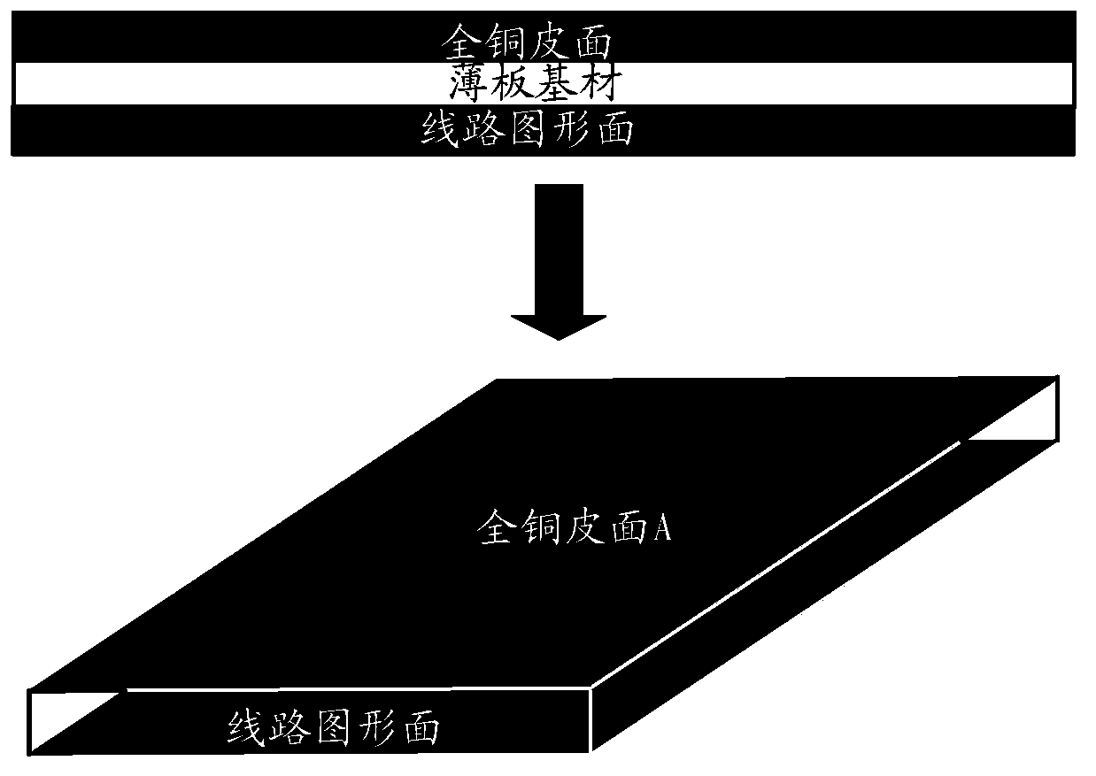
[0029] Step 101, making a sub-board of the printed circuit board, the sub-board includes a full copper skin surface layer, a base material layer and a circuit pattern surface layer;

[0030] Step 102, browning the circuit graphic layer of the sub-board;

[0031] Step 103, stacking PP sheets and adjacent sub-boards on the circuit pattern surface layer of the sub-board in sequence, stacking copper foil on the full-copper skin surface layer of the sub-board, and then pressing them together;

[0032] Step 104, tearing off the copper foil.

[0033] Because the method of the embodiment of the present invention uses copper foil to isolate the contact between th...


PUM


Abstract

The invention provides a manufacturing method of a PCB (Printed Circuit Board). The manufacturing method comprises the following steps: manufacturing sub-boards of the PCB, wherein each sub-board comprises a full-copper sheet surface layer, a substrate layer and a circuit pattern surface layer; performing brown oxidation on the circuit pattern surface layers of the sub-boards; sequentially stacking a PP (Propene Polymer) sheet and adjacent sub-boards on the circuit pattern surface layers of the sub-boards, stacking copper foils on the full-copper sheet surface layers of the sub-boards and then laminating; tearing off the copper foils The invention also provides a PCB which is manufactured by use of the method. The method can be used for improving the PCB manufacturing quality.

Description

technical field [0001] The present invention relates to the technical field of PCB (Printed Circuit Board, printed circuit board), in particular to a printed circuit board and a manufacturing method thereof. Background technique [0002] With the continuous upgrading of electronic products, the circuit density is getting higher and higher, and the circuit design has higher and higher requirements for PCB heat dissipation and power consumption. Many passive devices are integrated in the PCB. The application of embedded capacitor technology has made great progress. [0003] A major feature of buried capacitor materials is that the dielectric layer is relatively thin, generally below 25um. For the production of PCB products with thinner inner sub-boards, single-sided sequential etching and sequential lamination processes are usually used. This process uses two productions for the graphics on both sides of the same sub-board. The first time the first side is made, the second T...

Claims


Application Information

Patent Timeline
Patent Type & Authority Applications(China)
IPC IPC(8): H05K3/46H05K1/02
CPCH05K3/4617H05K3/4626H05K2203/06
Inventor 刘丰
Owner PEKING UNIV FOUNDER GRP CO LTD
Why Eureka
Try Eureka