
High-speed ADC (Analog to Digital Converter) sampled data receiving and buffering method and system based on FPGA (Field Programmable Gate Array)
A sampling data and data technology, applied in the direction of electrical digital data processing, instruments, etc., can solve the problems of inability to record data before triggering, low sampling data storage speed, short recording time, etc., and achieve fast speed, easy processing, and control simple effect
- Summary
- Abstract
- Description
- Claims
- Application Information
AI Technical Summary
Problems solved by technology
Method used
Image

Examples
Embodiment Construction
[0066] In order to make the method and technical solution of the present invention intuitive and easy to understand, the present invention will be further described in conjunction with the following specific embodiments and with reference to the accompanying drawings.
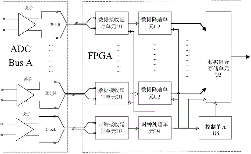
[0067] The present invention provides a method and system for receiving and buffering high-speed ADC sampling data based on FPGA. The system mainly includes the following components: a data receiving delay unit U1, a data deceleration unit U2, a clock receiving delay unit U3, and a clock processing unit U4. Data combination storage unit U5, control unit U6, see structure composition figure 1 .
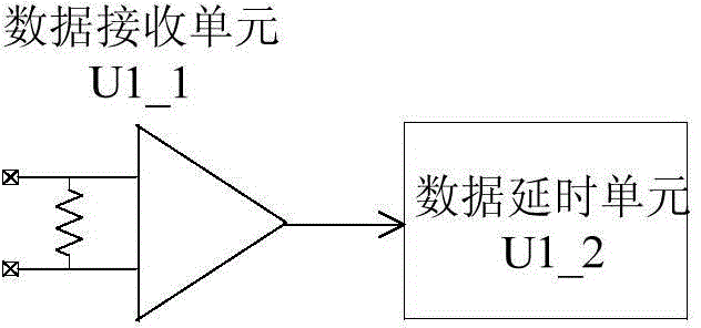
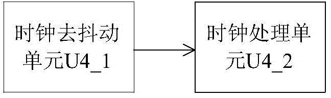
[0068] Among them, the data reception delay unit U1 realizes data reception and delay adjustment; the data deceleration unit U2 realizes the serial-to-parallel conversion of data signals, widening and deceleration; the clock reception delay unit U3 realizes the reception of the clock, and the coarse delay Timing adjust...
PUM
 Abstract
Description
Claims
Application Information