Method for verifying scrambled address of chip storage unit

A technology of storage unit and verification method, applied in static memory, instrument, etc., can solve the problems of low success rate, long analysis cycle, low efficiency, etc., and achieve the effect of improving the success rate and reducing the sample preparation cycle

Active Publication Date: 2018-02-06
SHANGHAI HUAHONG GRACE SEMICON MFG CORP
View PDF5 Cites 0 Cited by
  • Summary
  • Abstract
  • Description
  • Claims
  • Application Information

AI Technical Summary

Problems solved by technology

[0006] 3. The storage unit of the above-mentioned sample chip is bombarded by laser or focused ions, causing the failure of the storage unit at a specific position
[0011] 1. Destroy the interior of the sample at a fixed point by external force such as laser or focused ion bombardment. Due to the dense metal wiring on the upper layer of the chip, it is easy to cause the failure of the entire chip or the failure of a large area inside the memory, resulting in inaccurate positioning and a low success rate for completing the ideal sample. high
[0012] 2. In order to specifically confirm the actual physical address of the damage in the above step 5, it is necessary to peel off the layer by layer of the sample by grinding and chemical methods, until the internal structure can be seen, the address can be calculated, the efficiency is relatively low, and the analysis cycle is relatively long
[0013] 3. In order to confirm Article 2, fragments must be broken, resulting in waste of resources

Method used


Image

  • Method for verifying scrambled address of chip storage unit
  • Method for verifying scrambled address of chip storage unit
  • Method for verifying scrambled address of chip storage unit

Examples


Embodiment Construction

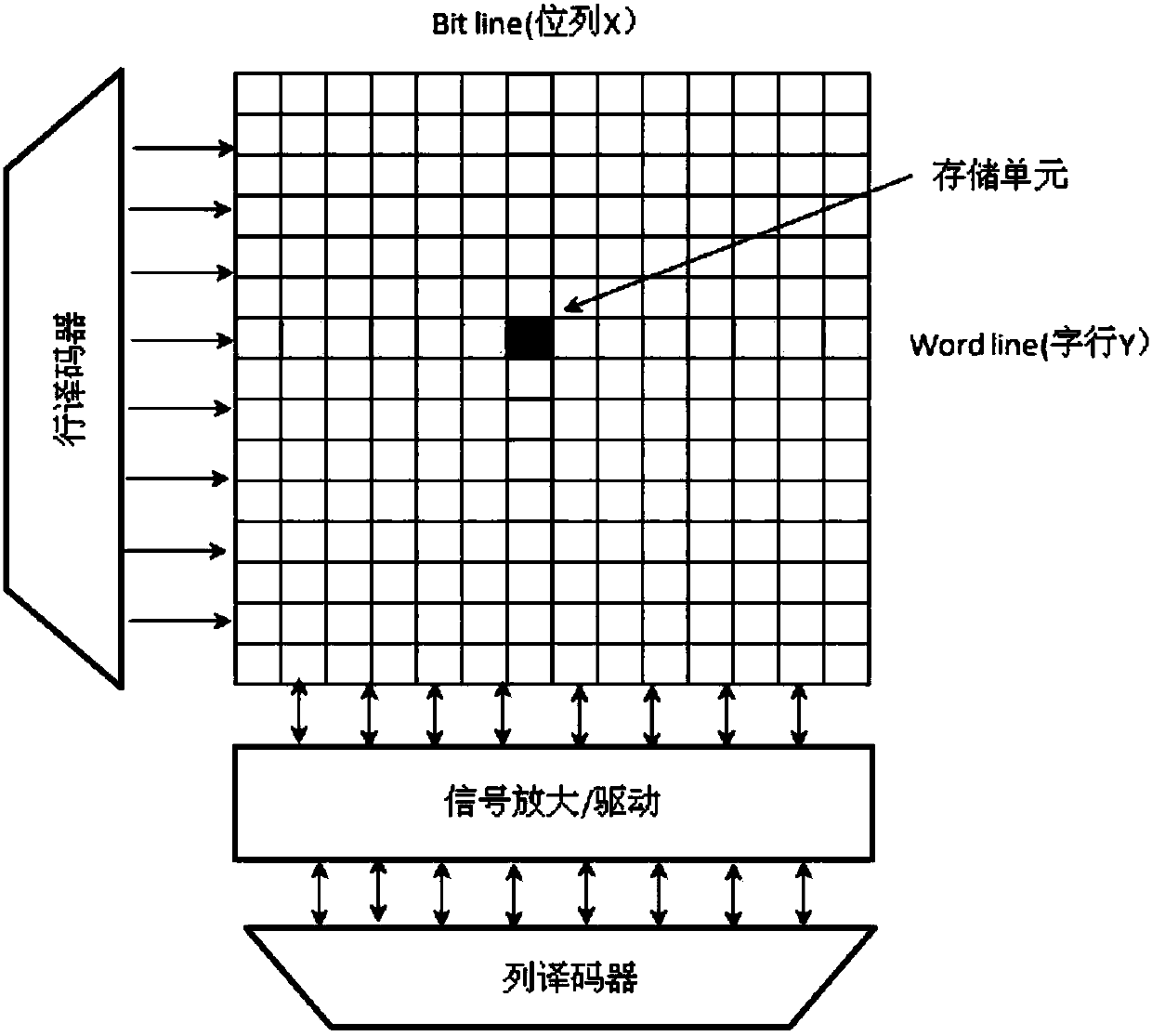
[0032] The method for verifying the scrambled address of the chip storage unit of the present invention includes the following steps:

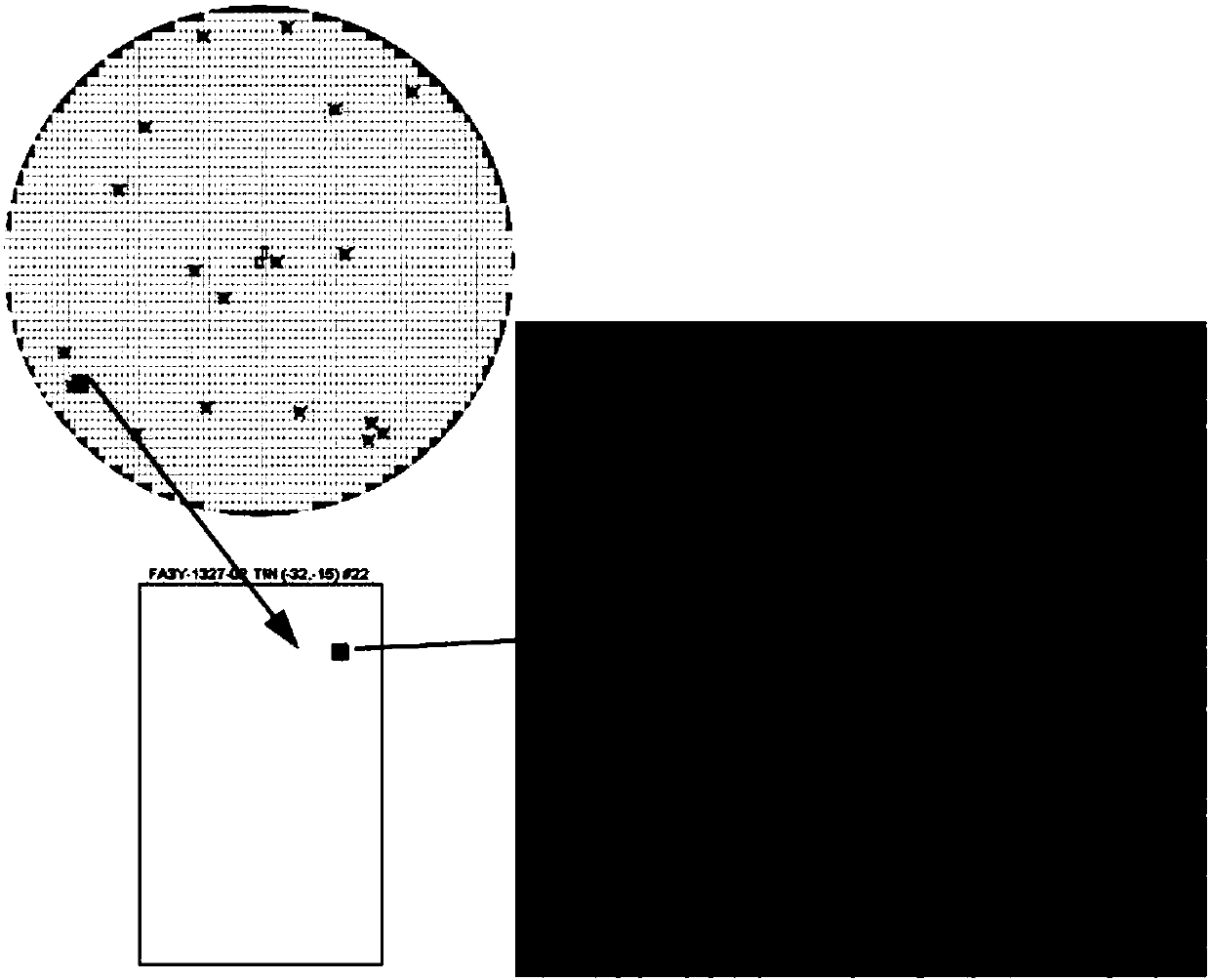
[0033] In the first step, in the process of mass production of the chip, the failure defect inside the memory is captured in the online defect detection.

[0034] Use the fatal flaws captured in the online inspection of the target product to perform post-scrambling address verification. On-line (silicon wafer production process) defect detection is a necessary step in the chip manufacturing process. The purpose is to: firstly catch the abnormality of the equipment or process in time to prevent the abnormal expansion; secondly, if there is a possibility of rework, rework in time to save losses . Utilizing the irreparable fatal defects that fall in the memory area, these fatal defects can be clarified in the storage area when they are caught, which is convenient for recording and later use.

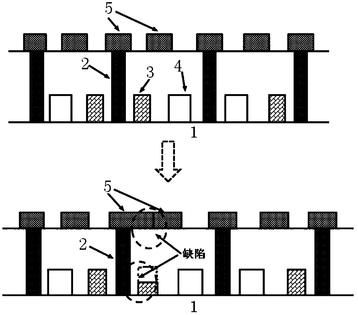
[0035] In addition, or using a focused ion beam to bombard...


PUM


Abstract

The invention discloses a method for verifying the scrambling code address of a chip storage unit, which includes: the first step, during the mass production process of the chip, the failure defect inside the memory is captured in the online defect detection or the defect is artificially manufactured by means of focused ion bombardment or the like lead to memory failure; the second step is to record the address of the failed chip on the wafer and the physical address of the failed defect in the storage unit; the third step is to continue to complete the chip manufacturing; the fourth step is to conduct ordinary electrical tests to obtain the failure The electrical address of the unit; the fifth step, write the conversion formula according to the memory structure design and test principle to obtain the physical failure address; the sixth step, compare the above physical failure address with the physical failure address recorded in the second step. The method does not need fragments to confirm the physical address, shortens the sample preparation period, and improves the success rate of verifying the scrambled code address of the storage unit.

Description

Technical field [0001] The invention relates to the field of integrated circuit manufacturing, in particular to a method for verifying the scrambling code address of a chip storage unit. Background technique [0002] Based on the design principle of the memory chip, the storage operation of the unit is performed through the electrical address, and the corresponding relationship with the actual physical address is more complicated. Therefore, in the failure analysis stage, the complex electrical address needs to be converted into a physical address that can find the failure point. To locate the failure site. This work requires the test engineer to write a fixed conversion formula in advance according to the design principle, and use laser or focused ion bombardment to destroy the internal structure of the sample to verify the correctness of the conversion formula. [0003] The specific method is as follows: [0004] 1. According to the design principle, find out the corresponding fo...

Claims


Application Information

Patent Timeline
Patent Type & Authority Patents(China)
IPC IPC(8): G11C29/56
Inventor 吴苑
Owner SHANGHAI HUAHONG GRACE SEMICON MFG CORP
Why Eureka
Try Eureka