Semiconductor device and method of forming the same

A technology of semiconductors and devices, which is applied in the field of semiconductor devices and their formation, can solve the problems that semiconductor devices are difficult to meet, and achieve the effects of reducing variation, improving radio frequency characteristics, and strong anti-interference ability

Active Publication Date: 2017-12-08
SHANGHAI HUAHONG GRACE SEMICON MFG CORP
View PDF3 Cites 2 Cited by
  • Summary
  • Abstract
  • Description
  • Claims
  • Application Information

AI Technical Summary

Problems solved by technology

[0003] However, today’s market requirements for chip performance are gradually increasing. For example, in the field of radio frequency communications, the market requires the chip’s anti-interference ability against radio frequency signals to be enhanced, and the accuracy of the chip’s signal transmission should also be improved; while relying on existing silicon-on-insulator technology manufacturing Semiconductor devices have become increasingly difficult to meet these demands

Method used


Image

  • Semiconductor device and method of forming the same
  • Semiconductor device and method of forming the same
  • Semiconductor device and method of forming the same

Examples


Embodiment Construction

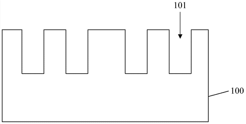
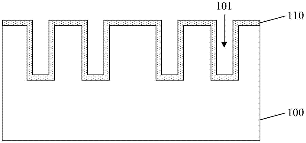
[0039] In the prior art, due to the buried oxide layer isolation between the silicon substrate and the top silicon (top silicon) in the SOI silicon wafer structure, there will be an inherent capacitance between the silicon substrate and the top silicon. In some cases, The passing radio frequency signal may interfere with the substrate below the buried oxide layer, causing the accumulation, depletion and even inversion of carriers in the substrate, and making the silicon substrate and the silicon substrate above the silicon substrate between the substrate and the top layer of silicon. Capacitance between regions where devices are formed will produce irregular and non-linear changes with radio frequency signals, thereby causing distortion of signal waveforms passing through semiconductor devices. Since these distortions or errors are usually non-linear and difficult to correct, it is necessary to improve the anti-interference ability of semiconductor devices.

[0040] To this en...


PUM


Abstract

The invention provides a semiconductor device and a forming method thereof. The forming method of the semiconductor device includes: providing first and second wafers; forming a plurality of trenches; forming a first oxide layer on the second wafer; The circle is bonded to the first wafer, the first wafer is used as the substrate of the semiconductor device, the first oxide layer is used as the buried oxide layer, and the second wafer is used as the top silicon for forming the device. The semiconductor device includes: a substrate; a second oxide layer located on the surface of the substrate; a first oxide layer; the first and second oxide layers together form a buried oxide layer; a first side of the substrate opposite to the buried oxide layer There are a plurality of trenches; the semiconductor device also includes a top layer of silicon formed on the buried oxide layer. The beneficial effect of the present invention is that the carriers accumulated on the surface of the substrate close to the buried oxide layer will be blocked by the trench, reducing the impact of the carriers on the capacitance, thereby reducing the variable capacitance of the interface under the buried oxide layer. With the amount of change, the radio frequency characteristics of the semiconductor device are improved.

Description

technical field [0001] The invention relates to the field of semiconductor manufacturing, in particular to a semiconductor device and a forming method thereof. Background technique [0002] In the field of radio frequency communication, silicon on insulator (Silicon On Insulator, SOI) technology has been widely used in order to optimize the radio frequency characteristics of semiconductor devices. The specific SOI technology is to isolate the silicon substrate silicon from the top layer silicon used to form semiconductor devices by forming a buried oxide layer. [0003] However, today’s market requirements for chip performance are gradually increasing. For example, in the field of radio frequency communications, the market requires the chip’s anti-interference ability against radio frequency signals to be enhanced, and the accuracy of the chip’s signal transmission should also be improved; while relying on existing silicon-on-insulator technology manufacturing Semiconductor...

Claims


Application Information

Patent Timeline
Patent Type & Authority Patents(China)
IPC IPC(8): H01L21/762
CPCH01L21/76251H01L24/83H01L21/764
Inventor 刘张李
Owner SHANGHAI HUAHONG GRACE SEMICON MFG CORP
Why Eureka
Try Eureka