
Planar gate IGBT with low-reverse transfer capacitance and anti-latch-up structure and manufacturing method of planar gate IGBT

A technology of reverse transmission and planar gate, which is applied in semiconductor/solid-state device manufacturing, circuits, electrical components, etc., can solve the problem of ineffective reduction of hole current flow path resistance, easy occurrence of LC oscillation, and insufficient P well concentration, etc. problem, achieve the effect of reducing the risk of LC oscillation, suppressing latch-up, and reducing the reverse transmission capacitance

Active Publication Date: 2015-03-11
STATE GRID CORP OF CHINA +2
View PDF4 Cites 16 Cited by
  • Summary
  • Abstract
  • Description
  • Claims
  • Application Information

AI Technical Summary

Problems solved by technology

The concentration of the P well under the N+ region formed by one injection and one push junction is still not high enough to effectively reduce the resistance of the hole current flow path, and there is still a risk of latch-up under high current conditions such as short circuits
[0004] The switching speed of IGBT is finally reflected in the charging and discharging speed of the internal capacitance of the surface MOSFET structure. The thickness of the oxide layer above the JFET area affects the size of the reverse transmission capacitance. The larger the capacitance, the slower the discharge speed and the higher the device turn-off loss. At the same time, when the device is short-circuit tested, due to the parasitic inductance L of the test circuit, LC oscillation is prone to occur. The conventional method is to add a capacitor between the gate and the emitter, which brings inconvenience to the test.

Method used


Image

  • Planar gate IGBT with low-reverse transfer capacitance and anti-latch-up structure and manufacturing method of planar gate IGBT
  • Planar gate IGBT with low-reverse transfer capacitance and anti-latch-up structure and manufacturing method of planar gate IGBT

Examples


Embodiment Construction

[0033] The specific implementation manners of the present invention will be further described in detail below in conjunction with the accompanying drawings.

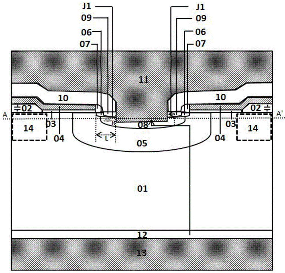
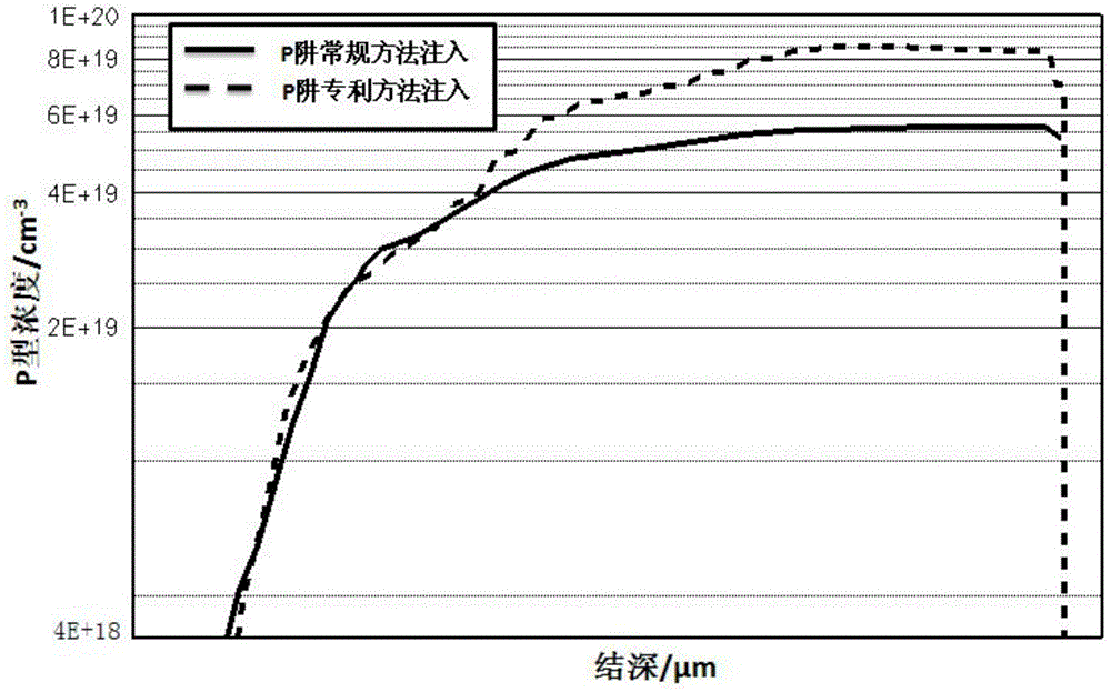
[0034]The present invention provides a planar gate IGBT with a low reverse transmission capacitance anti-latch-up structure. The planar gate IGBT includes a substrate 01, a field oxide layer 02 and a gate oxide layer 03 on the surface of the substrate, deposited on the gate oxide layer The polysilicon gate 04 on 03 and the P well region 05 between the gate oxide layer 03 and the substrate 01, the N well region 06 located on the surface of the P well region 05, and the P+ type in the P well region 05 are sequentially arranged from bottom to top The doped region 08 and the N+ type doped region 09, the JFET region is located between two P well regions 05; the P well region 05 is formed by multiple implantation and push junction processes, and the total implantation dose is between 6E13-8E13, A field oxide layer 02 is grown ...


PUM

PropertyMeasurementUnit
Thicknessaaaaaaaaaa

Abstract

The invention relates to a planar gate IGBT (Insulated Gate Bipolar Transistor) with a low-reverse transfer capacitance and anti-latch-up structure and a manufacturing method of the planar gate IGBT. P well injection is improved on the basis of a conventional method, and a P well multi-injection and multi-junction pushing mode is adopted under the condition of keeping total P well injection dose and total well pushing time unchanged, so that P well concentration below an N+ region is higher, the resistance of a path through which hole current flows can be reduced more effectively, the phenomenon of latch-up of an IGBT device in a high-current state can be effectively suppressed, and on-state voltage drop can also be reduced along with the reduction of the resistance. A layer of field oxide layer with a thickness of 1.0 to 1.5 microns is additionally arranged above a JFET (Junction Field-effect Transistor) region, so that the reverse transfer capacitance of the IGBT device is reduced, the discharge time of the reverse transfer capacitance when the device is turned off is shortened, and turning-off loss is reduced; the aim of avoiding LC oscillation during a short-circuit test can also be fulfilled by reducing the reverse transfer capacitance of the IGBT device.

Description

technical field [0001] The invention relates to a power semiconductor device and a manufacturing method thereof, in particular to a planar gate IGBT with a low reverse transmission capacitance anti-latch structure and a manufacturing method thereof. Background technique [0002] Power semiconductor devices are the core components to realize the transmission, conversion and process control of electric energy. It makes electric energy more efficient, more energy-saving, and more environmentally friendly, and turns "crude electricity" into "fine electricity". basic and core technologies. In the new generation of power semiconductor devices, because the insulated gate bipolar transistor (IGBT) device has the advantages of both unipolar devices and bipolar devices, the driving circuit is simple, the power consumption and cost of the control circuit are low, and the on-state voltage drops. Its own loss is small, so that IGBT devices have become the preferred devices in high-power...

Claims


Application Information

Patent Timeline
IPC IPC(8): H01L29/739H01L21/331H01L29/423H01L21/265
CPCH01L21/265H01L29/66325H01L29/7393
Inventor 高明超王耀华赵哿刘江金锐温家良
Owner STATE GRID CORP OF CHINA
Features
  • Generate Ideas
  • Intellectual Property
  • Life Sciences
  • Materials
  • Tech Scout
  • Unparalleled Data Quality
  • Higher Quality Content
  • 60% Fewer Hallucinations
Learn More