

Diode with floating island structure
A diode and floating island technology, applied in the field of power semiconductor devices, can solve the problems of increasing the conduction voltage drop, etc., and achieve the effects of reduced conduction voltage, short reverse recovery time, and good temperature characteristics
- Summary
- Abstract
- Description
- Claims
- Application Information
AI Technical Summary
Problems solved by technology
Method used
Image

Examples
Embodiment 1
[0023] Such as Figure 4 As shown, this example includes a cathode 7, an N-type semiconductor substrate 6 located on the upper layer of the cathode 7, an N-type semiconductor drift region 5 located on the upper layer of the N-type semiconductor substrate 6, and a gate oxide layer located on the upper layer of the N-type semiconductor drift region 5 2 and the anode 1 located on the upper layer of the gate oxide layer 2; the gate oxide layer 2 and the trench structure; an N-type semiconductor region 3 is arranged between the gate oxide layer 2 on both sides of the trench; in the N-type semiconductor drift region 5 is provided with a plurality of doped regions including P-type semiconductor doped regions 4 to form a floating island structure.
[0024] This example works as follows:
[0025] In the blocking state, the P-type floating island and the N-type semiconductor drift region 5 form a built-in potential, forming an electron potential barrier, which prevents electrons from f...
Embodiment 2
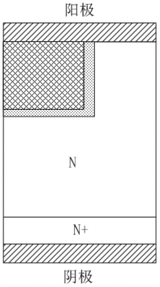
[0027] Such as Figure 5 As shown, the structure of this example is that a first heavily doped N-type semiconductor region 8 is arranged between the anode 1 and the N-type semiconductor region 3 on the basis of Embodiment 1. The working principle of this example is the same as that of Embodiment 1. The ohmic contact resistance can be further reduced.
Embodiment 3
[0029] Such as Figure 6 As shown, the structure of this example is that a second heavily doped N-type semiconductor region 9 is arranged between the anode 1 and the N-type semiconductor region 3 on the basis of Embodiment 2. The working principle of this example is the same as that of Embodiment 1. The ohmic contact resistance can be further reduced.
PUM
 Abstract
Description
Claims
Application Information