Method for confirming position alignment in wafer test

A wafer testing and wafer technology, which is applied in the field of confirmation of position alignment in wafer testing, can solve the problems of wasting wafer testing time, affecting product quality, and wrong wafer map position correspondence, and avoiding position The effect of shifting alignment, preventing position alignment errors, and saving test time

Active Publication Date: 2015-03-18
SHANGHAI HUAHONG GRACE SEMICON MFG CORP
View PDF13 Cites 16 Cited by
  • Summary
  • Abstract
  • Description
  • Claims
  • Application Information

AI Technical Summary

Problems solved by technology

[0003] As we all know, the camera system of the probe station has the minimum resolution. When the feature chip is too small, or the related parameters are set abnormally, or when the wafer has chromatic aberration during the manufacturing process, the probe station’s accuracy of the initial position of the wafer There will be deviations in the identification, which will lead to errors in the corresponding relationship between the wafer map and the actual wafer, resulting in a positional offset in the wafer map (such as image 3 shown)
If this situation is not discovered in time during wafer-level testing, it will lead to errors in the normal picking of chips in subsequent packaging tests. In serious cases, abnormal chips will be picked as good chips, which will seriously affect product quality.
In particular, chips at this stage are becoming more and more complex. There are more than 20,000 chips on a wafer, and there are often more than two testing procedures, such as high-temperature testing, normal temperature testing, low-temperature testing, specific project testing, and testing in a certain process. When an abnormality is found in the
If in a process test, the position of the wafer is identified incorrectly, it will seriously waste the wafer test time and affect the test quality of the chip

Method used


Image

  • Method for confirming position alignment in wafer test
  • Method for confirming position alignment in wafer test
  • Method for confirming position alignment in wafer test

Examples


Embodiment Construction

[0019] The method for confirming the position alignment in the wafer test of the present invention is to perform more than two test processes on the wafer containing the NVM IP (non-volatile memory Intellectual Property) chip Alignment confirmation method, its steps include:

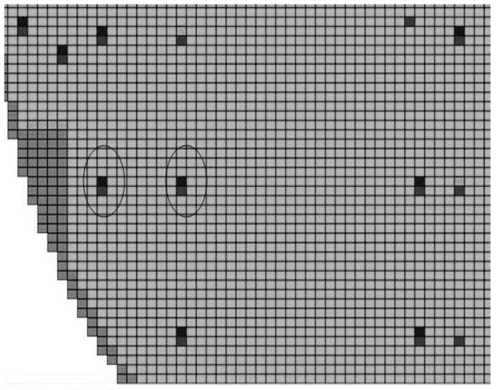
[0020] 1) First specify that the address Z in the memory area of ​​the chip is the location where the mapped address is stored. Address Z contains at least one byte; the chip also contains the chip status flag bit, which can be composed of one byte;

[0021] If the chip with the address Z area is normal, you can write information such as 0X5A in the flag bit. According to the needs, there is at least one target chip Tai, where "i" can be 1, 2, 3 and above. If there is one time, it is recorded as Ta1; if there are two, it is recorded as Ta1, Ta2; and so on.

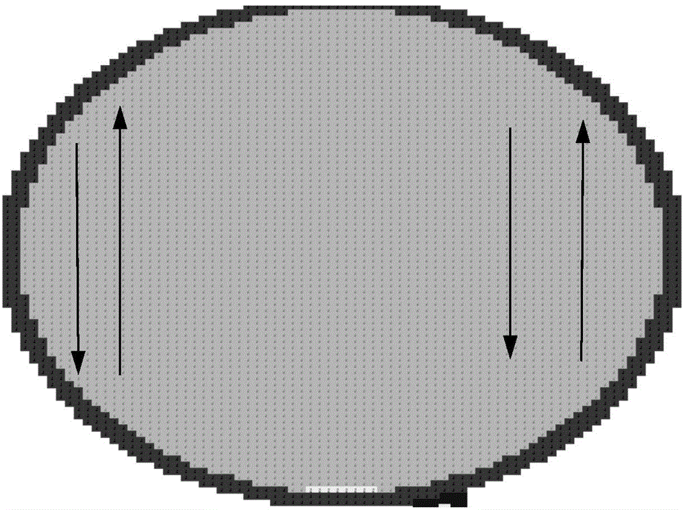
[0022] In order to improve the test efficiency, Tai position confirms that the target chip selection is often in the starting area of ​​the wafer chip te...


PUM


Abstract

The invention discloses a method for confirming position alignment in wafer test, comprising the following steps: (1) the position of an address Z in a chip memory area is specified as the position of storage mapping address, wherein a chip contains a chip status flag; (2) in the first test process, a tester reads information of a chip position A on a wafer from a prober system, and corresponding mapping relations are written into corresponding chips on the wafer through the tester; (3) in the second and subsequent process test, the chip position A read from the prober system is compared with a position A' read from a target chip, alarming is carried out through the tester if the two positions are not the same, and subsequent test continues if the two positions are consistent. Position alignment offset in multi-process test is avoided, the wafer test time is saved, and the quality of wafer test is guaranteed to the maximum.

Description

Technical field [0001] The invention relates to a position alignment method in the field of semiconductor testing, in particular to a confirmation method for realizing position alignment in wafer testing. Background technique [0002] In the existing semiconductor wafer-level testing, the testing of wafer chips relies on the probe system for position alignment and confirmation. In the test, when the wafer is transferred to the probe station chuck, the probe station system uses its internal camera system to identify the feature chips on the wafer to confirm the initial position. After the initial position is obtained, the test In, the probe station is set according to the expected wafer map (map) (such as figure 1 (Shown) to perform a needle stick test, or perform a needle stick test in a wafer map (map) according to the moving position sent by the tester. After the test is completed, you will get a map of the test results (such as figure 2 Shown). Subsequent inking or packagin...

Claims


Application Information

Patent Timeline
Patent Type & Authority Applications(China)
IPC IPC(8): G01R31/26
Inventor 谢晋春辛吉升
Owner SHANGHAI HUAHONG GRACE SEMICON MFG CORP
Why Eureka
Try Eureka