Radiating film substrate structure and manufacturing method thereof

A manufacturing method and heat-dissipating film technology, which are used in the manufacture of semiconductor/solid-state devices, electrical components, and electrical solid-state devices, etc., can solve problems such as defective products, influence on adhesion, and poor stability, and achieve improved thermal conductivity and heat dissipation efficiency. Efficiency, good bonding density

Inactive Publication Date: 2015-03-18
TENGRUI PHOTOELECTRIC TECH
View PDF3 Cites 1 Cited by
  • Summary
  • Abstract
  • Description
  • Claims
  • Application Information

AI Technical Summary

Problems solved by technology

[0004] (1) The heat dissipation film 2 is directly contacted with the ceramic plate 1, and the adhesion of the heat dissipation film 2 is poor
In detail, when the heat dissipation film material is sprayed on the high-temperature ceramic plate 1, it will produce a crystallization effect that is distributed on the ceramic plate 1. The crystallization must be controlled evenly and closely under the condition of extremely precise temperature and control. On the ceramic plate 1, in other words, the existing heat dissipation film substrate is bonded between the ceramic plate 1 and the heat dissipation film 2 without any other medium, so the manufacturing process must be carefully and accurately controlled, otherwise defective products will easily occur and the adhesion will be affected
[0005] (2) The material of the heat dissipation film 2 is only tin, antimony halides, and phosphorus compounds, and no other stabilizers (hydrochloric acid) and solvents (nitric acid) are added, so its stability is poor, which affects the effect of crystallization during spraying
[0006] (3) At low temperature (150°~160°C), the heat dissipation is poor (such as Figure 5 As shown), heat dissipation can only be achieved at a high temperature of 200°C, but the heating temperature of LED lamps is below 160°C, so the heat dissipation is poor for LED lamps

Method used


Image

  • Radiating film substrate structure and manufacturing method thereof
  • Radiating film substrate structure and manufacturing method thereof
  • Radiating film substrate structure and manufacturing method thereof

Examples


Embodiment Construction

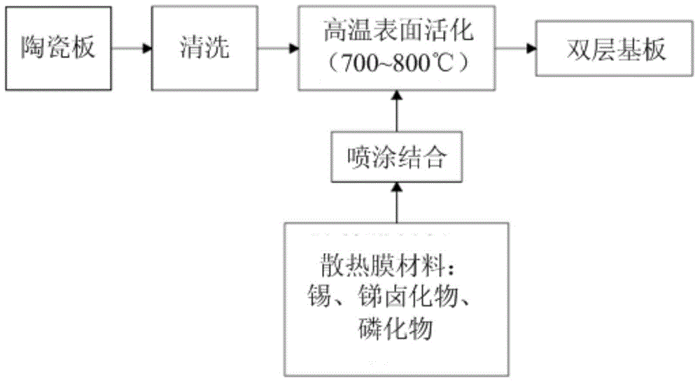
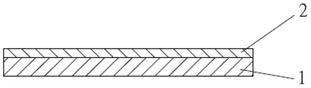
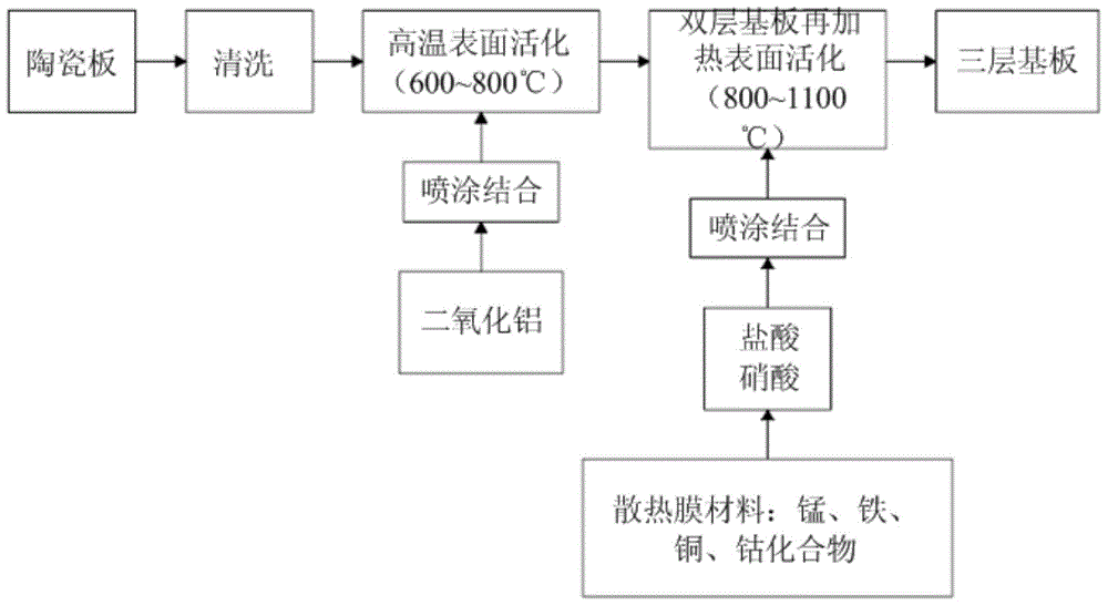
[0023] see image 3 , 4 , The manufacturing method process of the present invention includes: selecting materials, heating for the first time, spraying for the first time, heating for the second time, and spraying for the second time to form a three-layer substrate. The selected materials include: ceramic plate 10 as the substrate, silicon dioxide 11 as the dielectric layer, and manganese, iron, copper, cobalt compounds and other materials as the heat dissipation film 12 .

[0024] Firstly, the ceramic plate 10 is cleaned and dried, preheated at a high temperature of 600-800°C to activate the surface of the ceramic plate 10, and then the alumina 11 is sprayed and bonded to the surface of the ceramic plate 10 to form a double-layer substrate. The double-layer substrate is preheated at a high temperature of 800-1100°C, which also activates the surface of the aluminum dioxide 11, and then sprays the material of the heat dissipation film 12 on the surface of the alumina 11 to for...


PUM


Abstract

The invention relates to a radiating film substrate structure and a manufacturing method thereof, and provides a substrate with excellent radiating efficiency at high temperature and a manufacturing method thereof. The method mainly comprises the following steps: high-temperature surface activation is carried out on a ceramic plate for the first time; silica material is sprayed and combined to the surface of the ceramic plate to form a double-layer substrate; high-temperature surface activation is carried out on the substrate; and radiating film material is sprayed and combined to the surface of silica to form a three-layer radiating substrate, wherein the radiating film material is a mixture of manganese, iron, copper, cobalt compound, hydrochloric acid and nitric acid. By adopting silica, the adhesion can be enhanced, and the radiating film material does not fall off the ceramic plate. Hydrochloric acid and nitric acid can make the radiating film material stable. Through silica and the radiating film material, an excellent radiating effect can be achieved.

Description

technical field [0001] The invention relates to a heat dissipation film substrate structure and a manufacturing method thereof, which provides a heat dissipation film substrate with high heat dissipation efficiency and strong adhesion of heat dissipation film layers. Background technique [0002] Taking the heat dissipation treatment of light-emitting diodes (LEDs) as an example, in order to improve the heat dissipation effect, the light-emitting diodes are arranged on a substrate, and the heat conduction and heat dissipation are carried out through the substrate. Existing heat dissipation substrate and manufacturing method thereof: such as figure 1 , 2 As shown, a layer of heat dissipation film 2 is set on the ceramic plate 1. The formation of the heat dissipation film 2 is to clean the ceramic plate 1 and heat it at 700-800°C for pre-high temperature surface activation, and then spray the material of the heat dissipation film 2 on the surface for activation. The ceramic ...

Claims


Application Information

Patent Timeline
Patent Type & Authority Applications(China)
IPC IPC(8): H01L23/373H01L21/48H01L33/64
Inventor 张榳芳
Owner TENGRUI PHOTOELECTRIC TECH
Why Eureka
Try Eureka