

Substrate treatment device and device manufacturing method
A substrate processing device and substrate technology, which are applied to originals for photomechanical processing, exposure devices for photolithography, and instruments, can solve the problems of difficult to suppress the total cost and high cost of display panels, and achieve high precision Effects of projection exposure and high-efficiency exposure
- Summary
- Abstract
- Description
- Claims
- Application Information
AI Technical Summary
Problems solved by technology
Method used
Image

Examples
no. 1 Embodiment approach
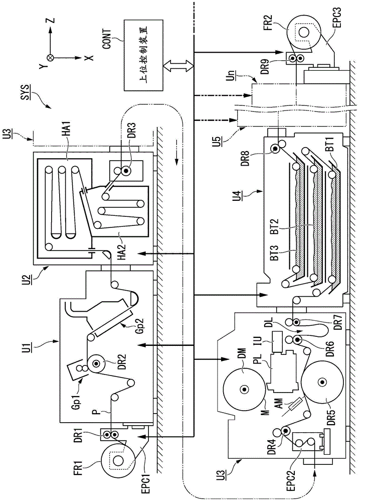
[0063] figure 1 It is a figure which shows the structure of an example of the device manufacturing system SYS (flexible display manufacturing line) of this embodiment. Here it is shown that the flexible substrate P (sheet, film, etc.) pulled out from the supply reel FR1 passes through n processing devices U1, U2, U3, U4, U5, ... Un in sequence until it is wound up in the recovery process. Example on reel FR2.
[0064] In the following description, regarding the XYZ rectangular coordinate system, the front surface (or back surface) of the substrate P is set to be perpendicular to the XZ plane and the width direction perpendicular to the conveyance direction (longitudinal direction) of the substrate P is set to be is the direction of the Y axis. In the following description, the rotation direction around the X-axis direction is referred to as the θX-axis direction, and similarly, the rotation directions around the Y-axis direction and the Z-axis direction are respectively refe...
no. 2 Embodiment approach
[0156] Next, a second embodiment will be described. In this embodiment, the same reference numerals are attached to the same components as those in the above-mentioned embodiment, and descriptions thereof are simplified or omitted.
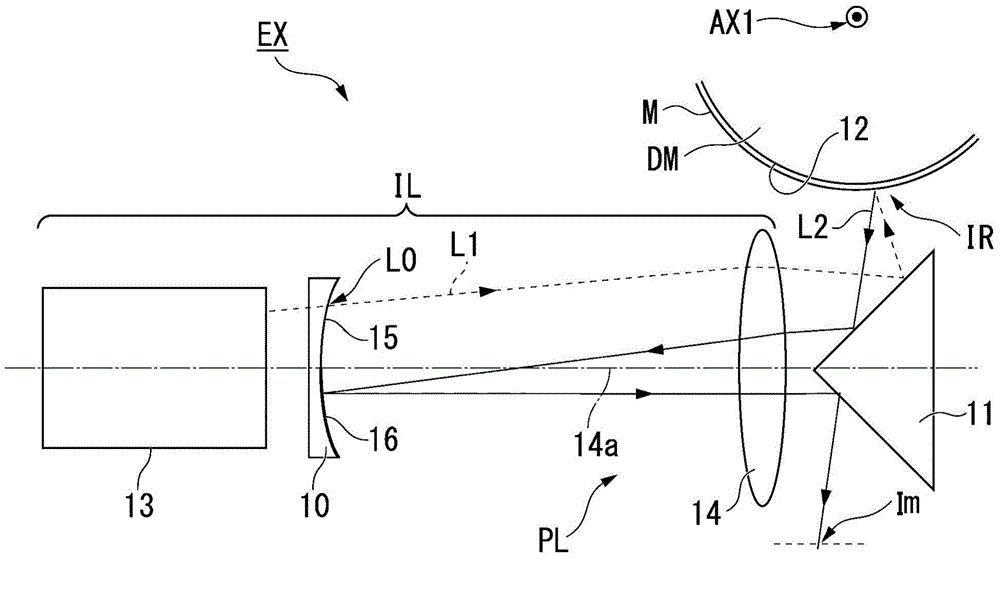
[0157] Figure 14 It is a figure which shows the structure of the processing apparatus (exposure apparatus EX2) of this embodiment. Figure 14 Exposure apparatus EX2 shown differs from 1st Embodiment in the point that projection optical system PL is comprised by the optical system like an Offner optical system.
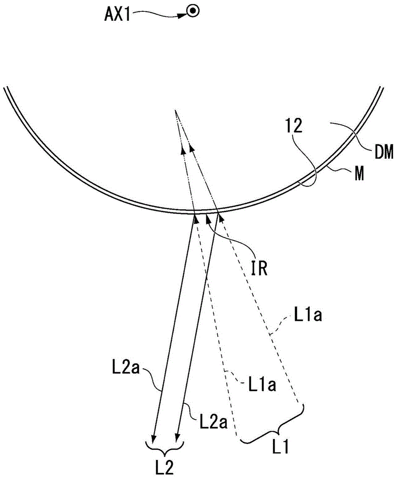
[0158] The projection optical system PL includes: a first projection optical system PL1 forming an intermediate image Im of a part (illumination region IR) of the mask pattern M; and a second projection optical system PL2 forming an intermediate image Im formed by the first projection optical system PL1 The projection area PR projected on the substrate P. Here, 1st projection optical system PL1 and 2nd projection optical system PL2 are...
no. 3 Embodiment approach
[0169] Next, a third embodiment will be described. In this embodiment, the same reference numerals are attached to the same components as those in the above-mentioned embodiment, and descriptions thereof are simplified or omitted.
[0170] Figure 16 It is a figure which shows the structure of the device manufacturing system SYS2 (flexible display manufacturing line) of this embodiment. Here, it is shown that the flexible substrate P (sheet, film, etc.) pulled out from the supply reel FR1 passes through n processing devices U1, U2, U3, U4, U5, ... Un in sequence until it is wound on Example on recycling reel FR2.
[0171] exist Figure 16 In , the XYZ orthogonal coordinate system is also set so that the surface (or back surface) of the substrate P is perpendicular to the XZ plane, and the direction (width direction) orthogonal to the conveyance direction (length direction) of the substrate P is set is the direction of the Y axis.
[0172] Next, the exposure principle of t...
PUM
| Property | Measurement | Unit |
|---|---|---|
| Thickness | aaaaa | aaaaa |
Abstract
Description
Claims
Application Information