
A device for producing silicon and silicon nitride nanoparticles

A nanoparticle and silicon nitride technology, which is applied in nanotechnology, nitrogen compounds, nanotechnology, etc. for materials and surface science, can solve the problems of low gas production rate, uneven distribution of electromagnetic field, and incapable of mass production, etc., and achieve improvement Productivity, the realization of large-scale industrial production, and the effect of increasing production

Active Publication Date: 2016-02-10
江西紫宸科技有限公司
View PDF4 Cites 0 Cited by
  • Summary
  • Abstract
  • Description
  • Claims
  • Application Information

AI Technical Summary

Problems solved by technology

However, the electromagnetic field distribution in the cavity of many devices that use the plasma method to produce nano-silicon particles is not uniform, which will reduce the productivity of the gas, cause waste of gas sources and environmental pollution, and also reduce the production of silicon nanoparticles. The distribution is relatively wide, and at the same time, it cannot be mass-produced, so that it cannot be industrialized
[0004] In addition, the preparation of silicon nitride by the self-propagating method has the advantages of energy saving and time saving, but the equipment requires high cost, high output and low output, so it cannot be industrialized
[0005] At present, the method for producing silicon nitride nanoparticles in the world is the direct nitriding method of silicon powder. This method has the advantages of simple process and low cost, but it also has the disadvantages of high firing temperature, long nitriding time, and serious waste of energy.

Method used


Image

  • A device for producing silicon and silicon nitride nanoparticles
  • A device for producing silicon and silicon nitride nanoparticles
  • A device for producing silicon and silicon nitride nanoparticles

Examples


Embodiment Construction

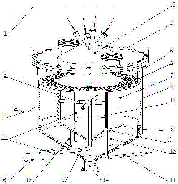
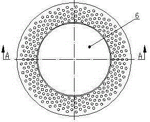
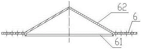
[0023] Description of reference signs: air inlet 1, observation window 2, anode 3, anode ground wire 4, polytetrafluoroethylene 5, quartz cover 6, solid cylinder 61, protruding cone 62, cathode 7, cathode wire 8, vacuum Electrode 9, cathode support 10, cooling water inlet 11, cooling water outlet 12, air inlet cover 13, air outlet 14, steel rod 15, cathode connection 16.

[0024] The present invention will be further described below in conjunction with the accompanying drawings.

[0025] This device is figure 1 As shown, the barrel-shaped outer wall is used as the anode 3, and the barrel can be made of stainless steel, that is, the anode 3 is made of stainless steel, and the inner surface of the barrel is covered with Si 3 N 4 (silicon nitride) coating. Such as figure 1 As shown, there are four symmetrically distributed gas inlets 1 on the air inlet cover 13 of the barrel-shaped outer wall, and the four air inlets 1 are arranged above the protruding cone on the air inlet...


PUM


Abstract

The invention relates to the field of silicon and silicon nitride nanoparticle production, in particular to a device for producing silicon and silicon nitride nanoparticle. The device of the present invention adopts that corresponding cones are arranged on the air inlet cover and the quartz cover, and the holes on the outer ring-shaped flat plate part on the quartz cover are reasonably distributed, so that the distribution of the plasma is uniform, and the size distribution of the nanoparticles is Narrower.

Description

Technical field [0001] The invention involves the production field of silicon and silicon nano -nanoparticles, and specially involves a device for the production of silicon and silicon nanoma. Background technique [0002] The nano structure has the characteristics of small size, larger area, and high surface energy. At the same time, it has three major effects: surface effects, small size effects, and macro quantum tunnel effects.Therefore, many characteristics that general materials are not available in aspects of optoelectronic and mechanics.Silicon nanoparticles have major applications in biological fluorescence markers, solar batteries, and lithium battery negative materials.Silicon nano -nanoparticles can be added to plastic or coatings as additives to greatly improve their mechanical strength and wear resistance, and can also reduce their friction coefficients. At the same timeIt has a good application as a high -temperature coating. [0003] At present, the method of prod...

Claims


Application Information

Patent Timeline
Patent Type & Authority Patents(China)
IPC IPC(8): C01B33/03C01B21/068B82Y30/00
Inventor 郑灵浪高志飞骆中伟
Owner 江西紫宸科技有限公司
Learn More