Charge pump circuit and storage device

A charge pump and circuit technology, applied in the direction of conversion equipment without intermediate conversion to AC, can solve the problem that it is difficult to meet the power requirements of the charge pump circuit, and achieve the effect of reducing power consumption

Inactive Publication Date: 2015-03-25
SHANGHAI HUAHONG GRACE SEMICON MFG CORP
View PDF7 Cites 12 Cited by
  • Summary
  • Abstract
  • Description
  • Claims
  • Application Information

AI Technical Summary

Problems solved by technology

[0010] However, the above method of reducing power is still difficult to meet the power requirements of the charge pump circuit in the standby state of the memory.

Method used


Image

  • Charge pump circuit and storage device
  • Charge pump circuit and storage device
  • Charge pump circuit and storage device

Examples


Embodiment Construction

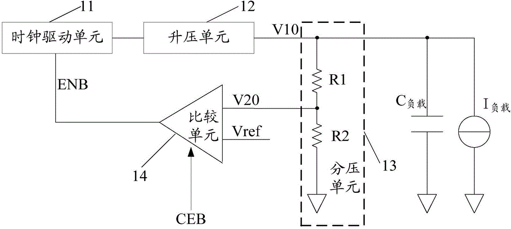
[0031] As mentioned in the background technology section, the charge pump circuit in the prior art has always used the resistor divider method, and the clock drive unit needs to work all the time. It is difficult to meet the requirements for the standby power of the charge pump circuit.

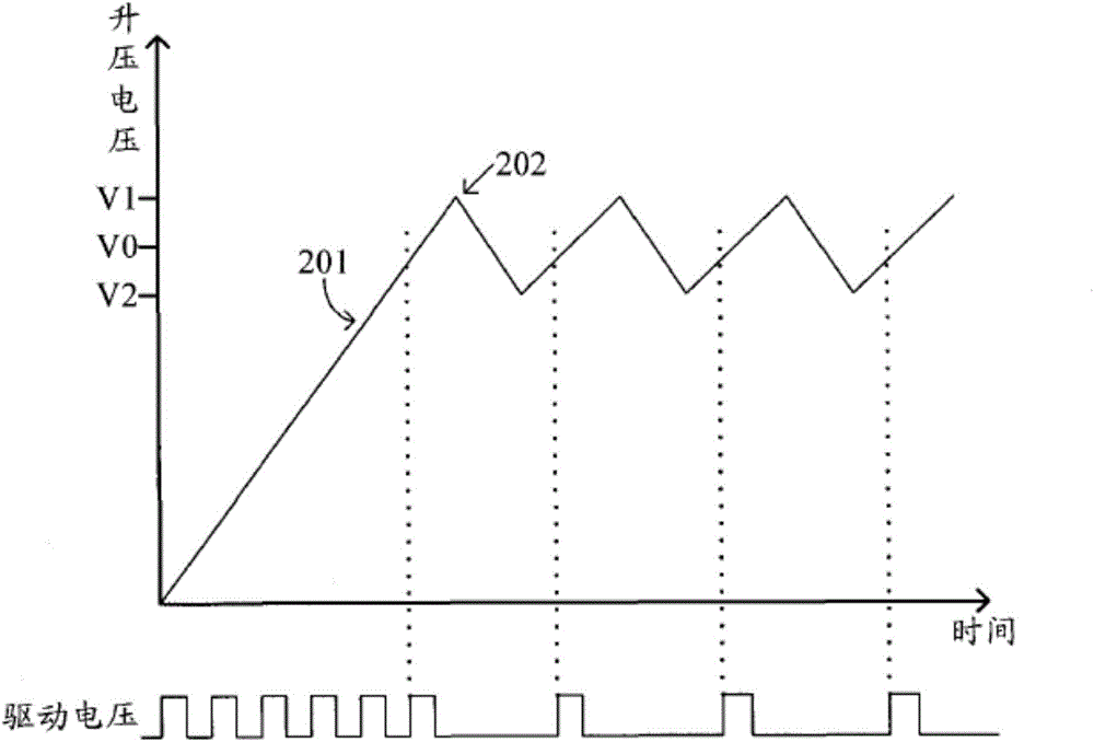
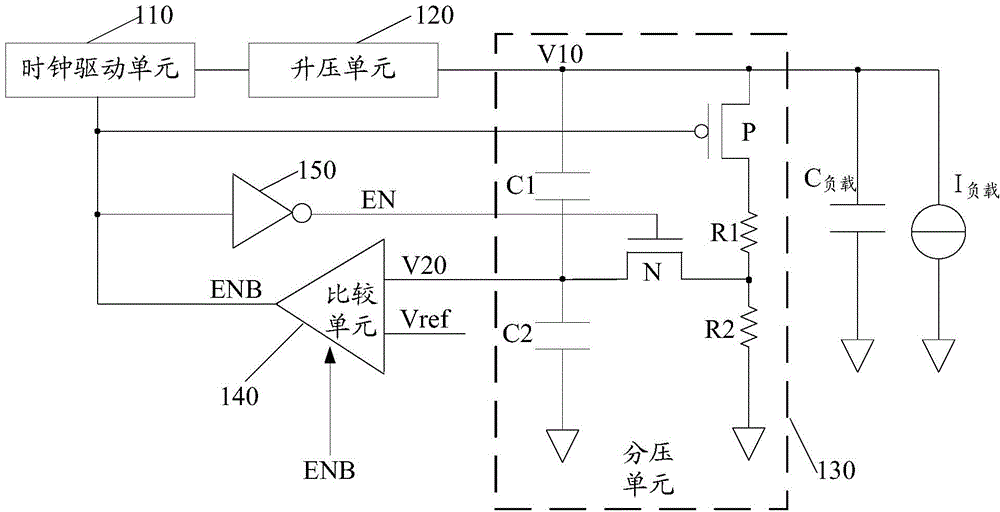
[0032]In view of the above technical problems, the present invention provides a charge pump circuit, including: a clock drive unit, a boost unit, a voltage divider unit and a comparison unit, wherein: the path from the comparison unit to the input end of the boost unit has a path delay, when the boosted voltage reaches the target voltage from the initial voltage, both the boosted voltage and the divided voltage change in a periodic oscillation, and when the divided voltage changes from a maximum value to a minimum value, the The comparison unit outputs the first control level, the clock drive unit and the non-capacitive voltage divider subunit stop working, and the capacitive voltage divider ...


PUM


Abstract

The invention discloses a charge pump circuit and a storage device. The charge pump circuit comprises a time clock driving unit, a boosting unit, a voltage dividing unit and a comparison unit. When receiving a first control level, the time clock driving unit stops working; otherwise, driving voltage is output; the boosting unit is used for boosting the driving voltage and then outputting boosted voltage; when the boosted voltage changes from the maximum voltage value to the minimum voltage value, a capacitance voltage dividing sub-unit divides the boosted voltage and outputs divided voltage; otherwise, a non-capacitance voltage dividing sub-unit divides the boosted voltage and outputs divided voltage; delay exits on the path from the comparison unit to the input end of the boosting unit, after the boosted voltage reaches target voltage from initial voltage, the boosted voltage and the divided voltage change in a periodic oscillation mode, and when the divided voltage changes from the maximum value to the minimum value, the comparison unit outputs the first control level; otherwise, a second control level is output. The power of the charge pump circuit can be effectively reduced.

Description

technical field [0001] The invention relates to the technical field of semiconductor memory, in particular to a charge pump circuit and memory. Background technique [0002] In recent years, during the rapid development of semiconductor memory, advanced memory such as DRAM, EFPROM, and FLASH has the advantages of high density, low power consumption, and low price, and it has become a storage device commonly used in computers and mobile communication terminals. In semiconductor memory, the charge pump circuit is a circuit module that provides high voltage, and the storage system uses the high-amplitude programming voltage drop output by the charge pump circuit to write data information into the memory module. [0003] figure 1 A schematic structural diagram of a charge pump circuit in the prior art is shown. The charge pump circuit includes: a clock drive unit 11, a boost unit 12, a voltage divider unit 13 and a comparison unit 14, wherein: in the start-up of the charge pum...

Claims


Application Information

Patent Timeline
Patent Type & Authority Applications(China)
IPC IPC(8): H02M3/07
CPCH02M3/07
Inventor 黄明永
Owner SHANGHAI HUAHONG GRACE SEMICON MFG CORP
Why Eureka
Try Eureka