Stacked semiconductor packaging method
A stacked packaging and semiconductor technology, applied in semiconductor devices, semiconductor/solid-state device manufacturing, electric solid-state devices, etc., can solve the problems of immature through-hole processing technology, inability to further reduce chip thickness, and high thickness, so as to save consumables , easy to operate, and the effect of increasing the conductive area
- Summary
- Abstract
- Description
- Claims
- Application Information
AI Technical Summary
Problems solved by technology
Method used
Image

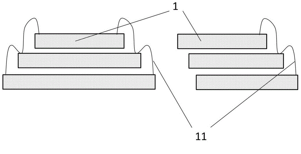
Examples
Embodiment Construction
[0042] The present invention will be described in further detail below in conjunction with the accompanying drawings and embodiments. It should be understood that the specific embodiments described here are only used to explain the present invention, not to limit the present invention.
[0043] In a first embodiment of the present invention, a semiconductor stack packaging method is provided. The method includes the following steps:
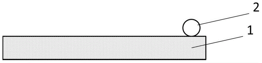
[0044] Form bumps on the chip. as attached figure 2 As shown, the bump 2 is formed on the chip 1, and the top of the bump 2 is preferably spherical or ellipsoidal. Those skilled in the art should understand that the top of the bump 2 can also be cylindrical or other shapes, figure 2 And other figures only illustrate the situation that the top of the bump is spherical.
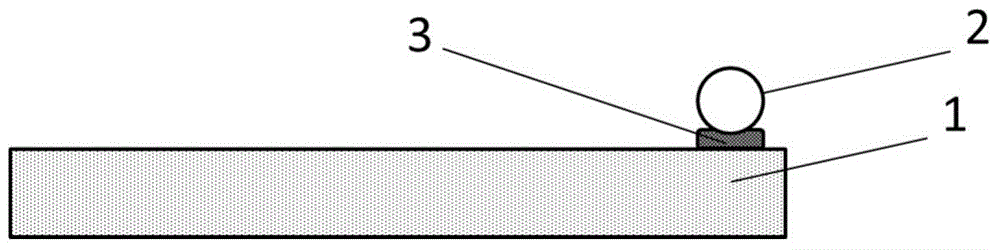
[0045] In another situation, such as image 3 As shown, there is a metal pad 3 (UBM) between the bump 2 and the chip, preferably, the metal pad 3 is an aluminum pad. The m...
PUM
 Abstract
Description
Claims
Application Information
 - Generate Ideas
- Intellectual Property
- Life Sciences
- Materials
- Tech Scout
- Unparalleled Data Quality
- Higher Quality Content
- 60% Fewer Hallucinations
Browse by: Latest US Patents, China's latest patents, Technical Efficacy Thesaurus, Application Domain, Technology Topic, Popular Technical Reports.
© 2025 PatSnap. All rights reserved.Legal|Privacy policy|Modern Slavery Act Transparency Statement|Sitemap|About US| Contact US: help@patsnap.com