Embedded sensing chip encapsulation structure with vertical through hole and manufacturing method thereof

A sensor chip and vertical through-hole technology, applied in the field of chip interconnection, can solve the problems of low yield, high cost of metal wiring, long-term reliability risks of products, etc., and achieve the effect of high reliability and low cost

Inactive Publication Date: 2015-04-01
HUATIAN TECH XIAN
View PDF9 Cites 22 Cited by
  • Summary
  • Abstract
  • Description
  • Claims
  • Application Information

AI Technical Summary

Problems solved by technology

The bonding pad of the sensor chip is located below the slope where the silicon substrate is located, avoiding the influence of the bonding wire on the distance between the sensing area and t

Method used


Image

  • Embedded sensing chip encapsulation structure with vertical through hole and manufacturing method thereof
  • Embedded sensing chip encapsulation structure with vertical through hole and manufacturing method thereof
  • Embedded sensing chip encapsulation structure with vertical through hole and manufacturing method thereof

Examples


Embodiment Construction

[0043] The invention will be further described below according to the accompanying drawings.

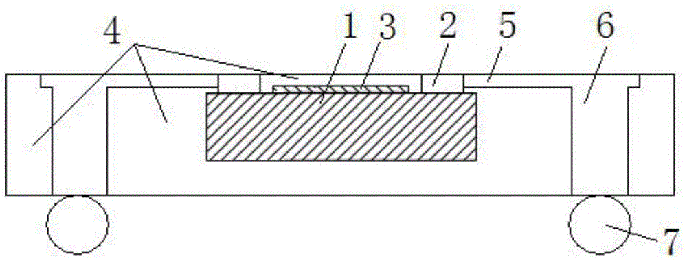
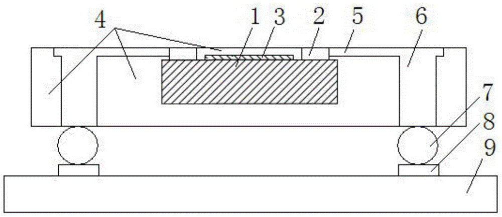
[0044] An embedded sensor chip packaging structure with vertical through holes, the structure includes a sensor chip 1, a sensor chip pad 2, a sensor structure part 3, a medium 4, a conductive line 5, and a through hole filled with a conductive material. holes 6, solder balls 7; the sensor chip 1 can be a fingerprint identification chip or other sensor chips, the sensor chip pad 2 is located on the top surface of the sensor chip 1, and the sensor structure part 3 is soldered to the sensor chip The disk 2 is located on the same surface, the side of the sensor chip 1 is covered with a medium 4, and there is a through hole 6 filled with a conductive material inside the medium 4, and the through hole 6 filled with a conductive material is connected with the conductive circuit 5 on the surface of the medium 4 and the conductive line 5 on the medium 4. The solder balls 7 on the back of the...


PUM

PropertyMeasurementUnit
Diameteraaaaaaaaaa

Abstract

The invention discloses an embedded sensing chip encapsulation structure with a vertical through hole and a manufacturing method of the embedded sensing chip encapsulation structure and belongs to the fields of integrated circuit encapsulation technologies, sensor technologies and the like. The manufacturing method comprises the steps that dielectric coating is performed on a complete sensor chip; wiring is performed on the surface of a dielectric, and the interior of the dielectric is drilled to be filled with conductive materials; a bonding pad on the surface of the sensor chip is led to a metal soldered ball on the reverse of the dielectric material and is interconnected with the outside through the metal soldered ball. According to the encapsulation structure, wiring is performed on the surface and the interior of the dielectric material, the operations like step etching on the sensor chip itself are avoided, and secondary encapsulation of surface-mounted glass, sapphire and other elements of the sensor chip is facilitated. Besides, through the structure, the cost is lowered, and the encapsulation yield and the reliability of products are improved.

Description

technical field [0001] The invention relates to technologies such as microelectronic package technology, sensor technology and chip interconnection. Background technique [0002] With the continuous improvement of the intelligence of terminal products, various sensor chips emerge in endlessly. Sensor chips have expanded the application fields of smart phones, tablet computers and other products. For example, the emergence of fingerprint recognition chips has greatly improved the security of the above products. [0003] For the sensor chip, its biggest feature is that there is a sensing area on the surface of the chip, which interacts with the external stimulus to be recognized to generate electrical signals that the chip can recognize and process. The distance between this area and external stimuli should be as short as possible so that the generated signal can be detected. In many current chip technologies, the chip pads are generally located on the same surface. If the c...

Claims


Application Information

Patent Timeline
IPC IPC(8): H01L23/488H01L23/498H01L23/49H01L21/60G06K9/00
CPCH01L21/568H01L2224/04105H01L2224/11H01L2224/19H01L2224/96
Inventor 庞诚于大全
Owner HUATIAN TECH XIAN
Why Eureka
Try Eureka