Manufacturing method and used etching method of complementary metal-oxide-semiconductor transistor (CMOS) imaging sensor

A technology of an image sensor and a manufacturing method, applied in radiation control devices and other directions, can solve the problems of lack of ideal and obvious notching, and achieve the effects of simple implementation, avoiding notching phenomenon, and easy promotion

Active Publication Date: 2013-05-08
ADVANCED MICRO FAB EQUIP INC CHINA
View PDF4 Cites 5 Cited by
  • Summary
  • Abstract
  • Description
  • Claims
  • Application Information

AI Technical Summary

Problems solved by technology

However, when applied to the etching process for manufacturing CMOS image sensors, especially when TSV technology is used, the above scheme does not have an ideal effect on the notching phenomenon, and the notching is still relatively obvious, such as figure 2 shown

Method used


Image

  • Manufacturing method and used etching method of complementary metal-oxide-semiconductor transistor (CMOS) imaging sensor
  • Manufacturing method and used etching method of complementary metal-oxide-semiconductor transistor (CMOS) imaging sensor
  • Manufacturing method and used etching method of complementary metal-oxide-semiconductor transistor (CMOS) imaging sensor

Examples


Embodiment Construction

[0027] The specific embodiment of the present invention will be further described in detail below in conjunction with the accompanying drawings.

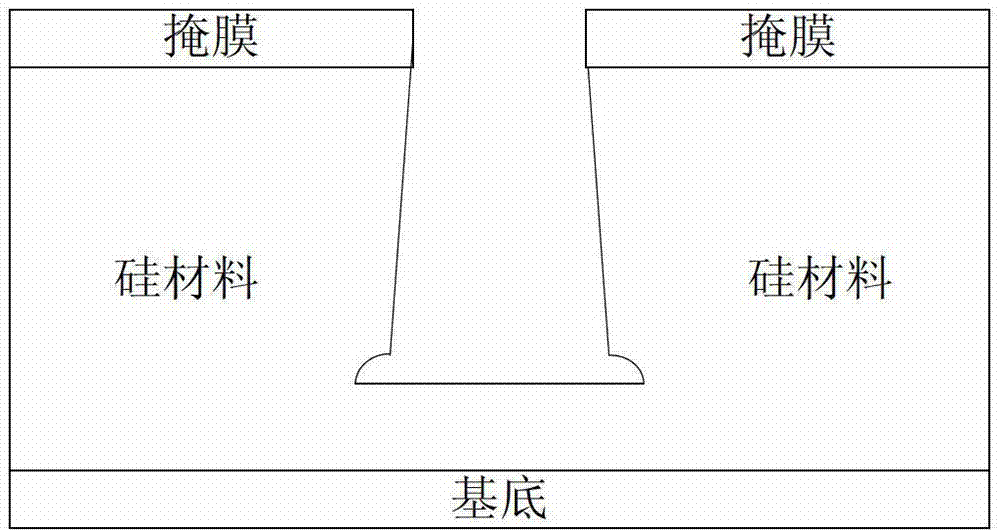
[0028] It should be noted that the embodiments of the present invention can be applied not only to the TSV etching process, but also to other etching processes for manufacturing CMOS image sensors.

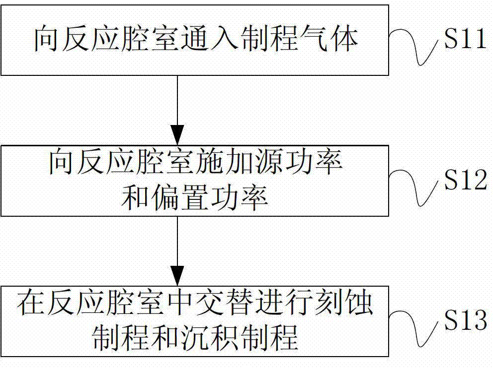
[0029] Such as image 3 As shown, the etching method for manufacturing a CMOS image sensor provided by the first embodiment of the present invention includes the following steps:

[0030] S11. Introducing a process gas into the reaction chamber, where the process gas includes an etching gas and a sidewall protection gas.

[0031] Specifically, a workpiece to be processed is placed in the reaction chamber, which is a semiconductor substrate with a pattern of shallow trenches defined therein, for manufacturing a CMOS image sensor. Etching gas including SF 6 and other gases that can cause etching reactions, sidewall protection gases inc...


PUM


Abstract

The invention relates to a manufacturing method and a used etching method of a complementary metal-oxide-semiconductor transistor (CMOS) imaging sensor. The etching method comprises the following steps: blowing manufacture procedure gas into a reaction cavity, wherein the manufacture procedure gas comprises etching gas and side wall protective gas; exerting source power and bias power to the reaction cavity, wherein the bias power varies in an impulse mode; and conducting an etching manufacture procedure and a deposit manufacture procedure in the reaction cavity in an alternate mode, wherein the source power is lower than 2,000 watt. By means of the manufacturing method and the used etching method of the CMOS imaging sensor, the phenomenon of notching can be effectively avoided, product yield can be improved, implementation is simple and popularization is easy.

Description

technical field [0001] The present invention relates to a semiconductor processing and manufacturing method, more specifically, to a manufacturing method of a CMOS image sensor and an etching method used therefor. Background technique [0002] CMOS image sensors can integrate pixel arrays and peripheral circuits on the same chip. Compared with charge-coupled devices, CMOS image sensors have the advantages of small size, light weight, low power consumption, convenient programming, easy control, and low average cost. [0003] In the prior art, the process of forming a CMOS image sensor refers to figure 1 To illustrate. Provide a semiconductor substrate 100 including a peripheral circuit area IA and a pixel unit area IB, the pixel unit area IB includes a photodiode area and a driver circuit area; then, a pad oxide layer 101 is formed on the semiconductor substrate 100 by a thermal oxidation method, and the pad oxide layer The material of layer 101 is silicon oxide; a barrier ...

Claims


Application Information

Patent Timeline
Patent Type & Authority Applications(China)
IPC IPC(8): H01L27/146
Inventor 卞祖洋
Owner ADVANCED MICRO FAB EQUIP INC CHINA
Why Eureka
Try Eureka