Capacitive touch panel and manufacturing method

A technology of capacitive touch and manufacturing method, which is applied in the direction of electrical digital data processing, instrumentation, input/output process of data processing, etc., can solve problems such as micro-short circuit and touch insensitivity, so as to prevent micro-short circuit and reduce the number of layers , cost reduction effect

Pending Publication Date: 2015-04-08
SHENZHEN LEAGUER OPTRONICS
View PDF3 Cites 3 Cited by
  • Summary
  • Abstract
  • Description
  • Claims
  • Application Information

AI Technical Summary

Problems solved by technology

Because Cu is easy to diffuse in the SiO2 film layer, when using a glass substrate, the SiO2 film layer will be used under the ITO film layer of the capacitive touch screen. Th

Method used


Image

  • Capacitive touch panel and manufacturing method
  • Capacitive touch panel and manufacturing method
  • Capacitive touch panel and manufacturing method

Examples


Embodiment Construction

[0015] In order to make the object, technical solution and advantages of the present invention clearer, the present invention will be further described in detail below in conjunction with the accompanying drawings and embodiments. It should be understood that the specific embodiments described here are only used to explain the present invention, not to limit the present invention.

[0016] The specific realization of the present invention is described in detail below in conjunction with specific embodiment:

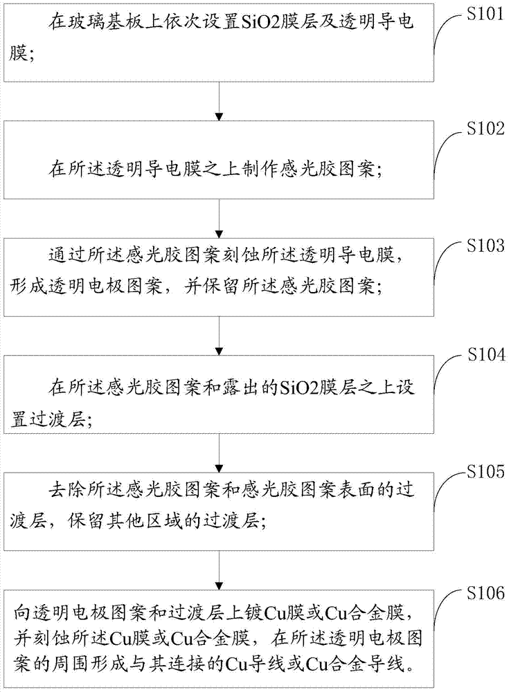
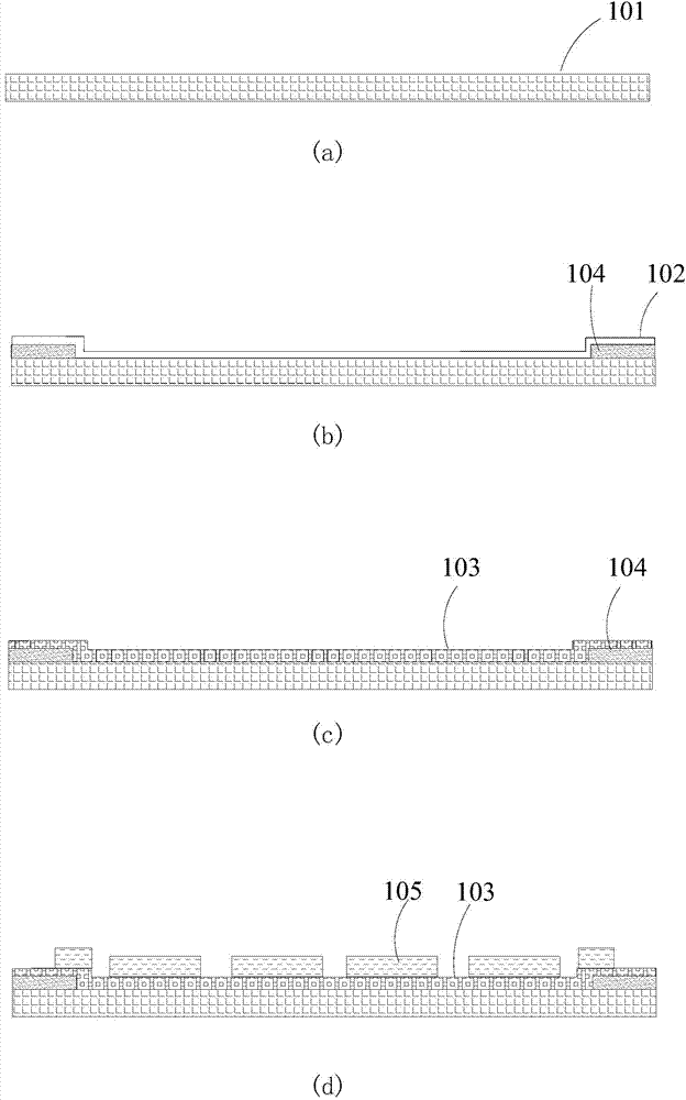
[0017] Please refer to figure 1 and figure 2 , an embodiment of the present invention provides a method for manufacturing a capacitive touch panel, comprising the following steps:

[0018] In step S101, the SiO2 film layer 102 and the transparent conductive film 103 are sequentially arranged on the glass substrate 101; figure 2 Figures (a), (b), (c) in Figure 1. The following figures do not show the structure of the SiO2 film layer 102 .

[0019] In this embodiment...


PUM

PropertyMeasurementUnit
Thicknessaaaaaaaaaa

Abstract

The invention applies to the technical field of touch, and provides a manufacturing method of a capacitive touch panel. The manufacturing method of the capacitive touch panel comprises the steps of sequentially arranging an SiO2 film layer and a transparent conductive film on a glass base plate; manufacturing a light sensitive glue pattern on the transparent conductive film; etching the transparent conductive film through the light sensitive glue pattern to form a transparent electrode, wherein the light sensitive glue pattern is remained; arranging a transition layer on the light sensitive glue pattern and the SiO2 film layer; removing the light sensitive glue pattern and the transition layer on the surface, and remaining the transition layer on the SiO2 film layer; coating a Cu film or a Cu alloy film on the transparent electrode pattern and the transition layer; etching the Cu film or the Cu alloy film; forming a Cu conductor around the transparent electrode pattern. The manufacturing method has the advantages that the Cu conductor and the SiO2 film layer are insulated through the transition layer, so that Cu elements are prevented from being dispersed to the SiO2 film layer, and as a result, micro short circuit of the transparent electrode can be prevented, the problem that the Cu material cannot be applied to the glass base plate can be overcome, the cost can be decreased, and the productivity and yield are improved.

Description

technical field [0001] The invention belongs to the field of touch technology, in particular to a capacitive touch panel and a manufacturing method. Background technique [0002] The structure of the capacitive touch screen is mainly to coat a layer of transparent ITO film conductor layer on the screen, and to plate narrow and long electrodes on the four sides of the touch screen to form a low-voltage AC electric field in the conductive layer. When touching the screen, a coupling capacitance will be formed between the finger and the conductor layer, and the current from the electrodes on the four sides will flow to the contact, and the current strength is proportional to the distance from the finger to the electrode, and the controller behind the touch screen will calculate the current. Proportion and strength, accurately calculate the position of the touch point. Because the surrounding electrodes are very thin, metal materials with low resistivity are required. MoAlMo or ...

Claims


Application Information

Patent Timeline
IPC IPC(8): G06F3/044
CPCG06F3/044
Inventor 黄亮余汉水刘锡钢陈凯孙伟杰蒋蔚
Owner SHENZHEN LEAGUER OPTRONICS
Why Eureka
Try Eureka