Microfluidic surface-enhanced Raman scattering transparent device structure and preparation method thereof

A surface-enhanced Raman and device structure technology, applied in Raman scattering, material excitation analysis, etc., can solve problems such as difficult to achieve effective bonding, numerous process steps, device detection failure, etc., to shorten detection time and improve signal-to-noise Ratio, the effect of improving consistency

Inactive Publication Date: 2015-04-15
JIANGSU CAS JUNSHINE TECH +1
View PDF2 Cites 12 Cited by
  • Summary
  • Abstract
  • Description
  • Claims
  • Application Information

AI Technical Summary

Problems solved by technology

However, the reported microfluidic SERS (Surface-enhanced Raman scattering) detection device has a complicated preparation process and involves many process steps, and its active substrate is generally prepared from materials that are opaque to visible light. During detection, the laser enters the device from the front, but often because the measured substance covers the nano-forest structure, the laser cannot pass through the ...

Method used


Image

  • Microfluidic surface-enhanced Raman scattering transparent device structure and preparation method thereof
  • Microfluidic surface-enhanced Raman scattering transparent device structure and preparation method thereof
  • Microfluidic surface-enhanced Raman scattering transparent device structure and preparation method thereof

Examples


Embodiment 1

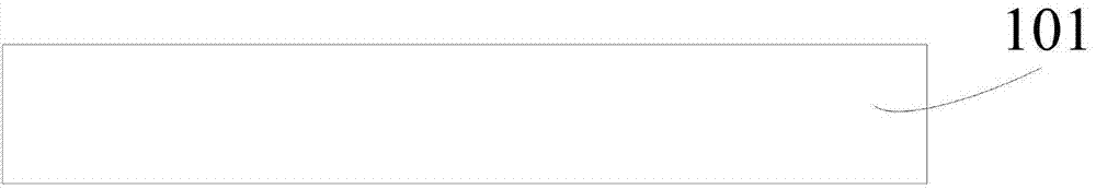
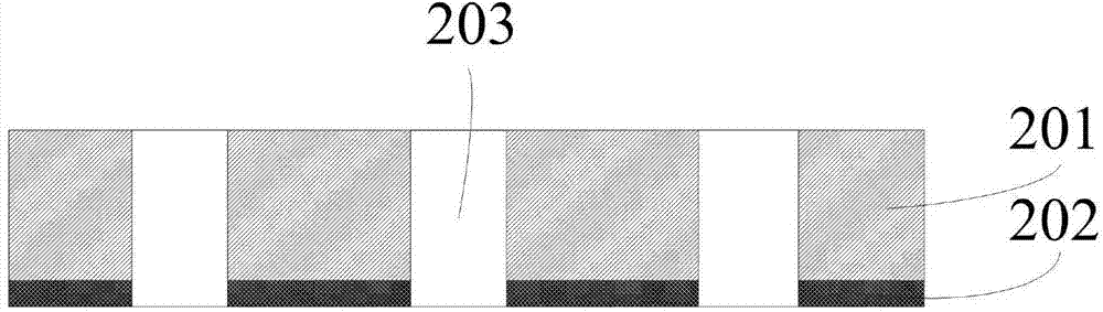
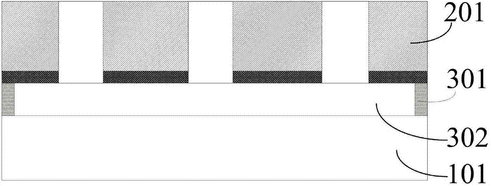
[0063] The first substrate 101 is made of glass material, the second substrate 201 is a glass sheet; the first microfluidic channel substrate 801 is made of a single crystal silicon wafer; the material of the microfluidic channel structure layer 1606 is polydimethylsiloxane. Among them, the first substrate 101 is used to finally obtain the metal nano-forest structure 601 on its surface; the second substrate 201 is used to realize the hollow structure; the first microfluidic channel substrate 801 is used to make the microfluidic channel mold 901 . The specific steps are:

[0064] Step 1. Prepare a surface-enhanced Raman scattering active substrate based on the metal nano-forest structure 601 on the first substrate 101, that is, prepare a transparent active substrate 1605, and set at least one metal nano-forest structure 601 on the transparent active substrate 1605.

[0065] The specific steps are:

[0066] 1-a. Prepare and clean the first substrate 101, the second substrate 20...

Embodiment 2

[0088] The first substrate 101 is a glass sheet; the second substrate 201 is a single crystal silicon sheet; the second microfluidic channel substrate 1301 is a glass sheet; the material of the microfluidic channel structure layer 1606 is glass. Among them, the first substrate 101 is used to finally obtain the metal nano-forest structure 601 on its surface; the second substrate 201 is used to realize the hollow structure; the second microfluidic channel substrate 1301 is used to make the microfluidic channel structure layer 1606 .

[0089] Step 1. Prepare a surface-enhanced Raman scattering active substrate based on the metal nano-forest structure 601 on the first substrate 101, that is, prepare a transparent active substrate 1605, and set at least one metal nano-forest structure 601 on the transparent active substrate 1605.

[0090] The specific steps are:

[0091] 1-a. Prepare and clean the first substrate 101, the second substrate 201 and the second microfluidic channel sub...


PUM

PropertyMeasurementUnit
Thicknessaaaaaaaaaa
Diameteraaaaaaaaaa
Heightaaaaaaaaaa

Abstract

The invention relates to a microfluidic surface-enhanced Raman scattering transparent device structure and a preparation method thereof. According to the technical scheme provided by the invention, the microfluidic surface-enhanced Raman scattering transparent device structure comprises a transparent active substrate and a microfluidic channel structure layer supported on the transparent active substrate, wherein a plurality of detection microfluidic channels are arranged inside the microfluidic channel structure layer; the detection microfluidic channels are communicated with a liquid inlet and a liquid outlet in the microfluidic channel structure layer; metal nano forest structures are arranged on the surfaces of areas of the transparent active substrate corresponding to the detection microfluidic channels; the metal nano forest structures are positioned between the liquid inlet and the liquid outlet. The microfluidic surface-enhanced Raman scattering transparent device structure is compact in structure and can improve the consistency of a surface-enhanced Raman scattering detection signal to shorten the detection time, can improve the signal-to-noise ratio of the surface-enhanced Raman scattering detection signal, can realize real-time detection of a variety of substances at the same time, and is wide in application range, safe and reliable.

Description

technical field [0001] The invention relates to a Raman scattering transparent device structure and a preparation method thereof, in particular to a microfluidic surface-enhanced Raman scattering transparent device structure and a preparation method thereof, belonging to the technical field of semiconductor devices. Background technique [0002] The detection technology based on Raman scattering spectroscopy is a method of material structure analysis that does not require labeling of the sample to be detected, and has the characteristics of non-destructive and contact-free. With the development of laser technology and weak signal detection and reception technology, as a means to realize the molecular level detection of material structure, Raman scattering spectroscopy detection technology is expected to obtain practical and practical results in the fields of biological detection, disease diagnosis, environmental monitoring, chemical analysis and so on. Wide range of applicat...

Claims


Application Information

Patent Timeline
IPC IPC(8): G01N21/65
CPCG01N21/65
Inventor 毛海央吴文刚欧文
Owner JIANGSU CAS JUNSHINE TECH
Why Eureka
Try Eureka